Electrical characteristics – Diodes APX324 User Manual
Page 5
APX321/APX358/APX324
LOW VOLTAGE, RAIL-TO-RAIL INPUT AND OUTPUT
SINGLE/DUAL/QUAD OPERATIONAL AMPLIFIERS
APX321/APX358/APX324 Rev. 13
5 of 18
FEBRUARY 2009
©
Diodes Incorporated
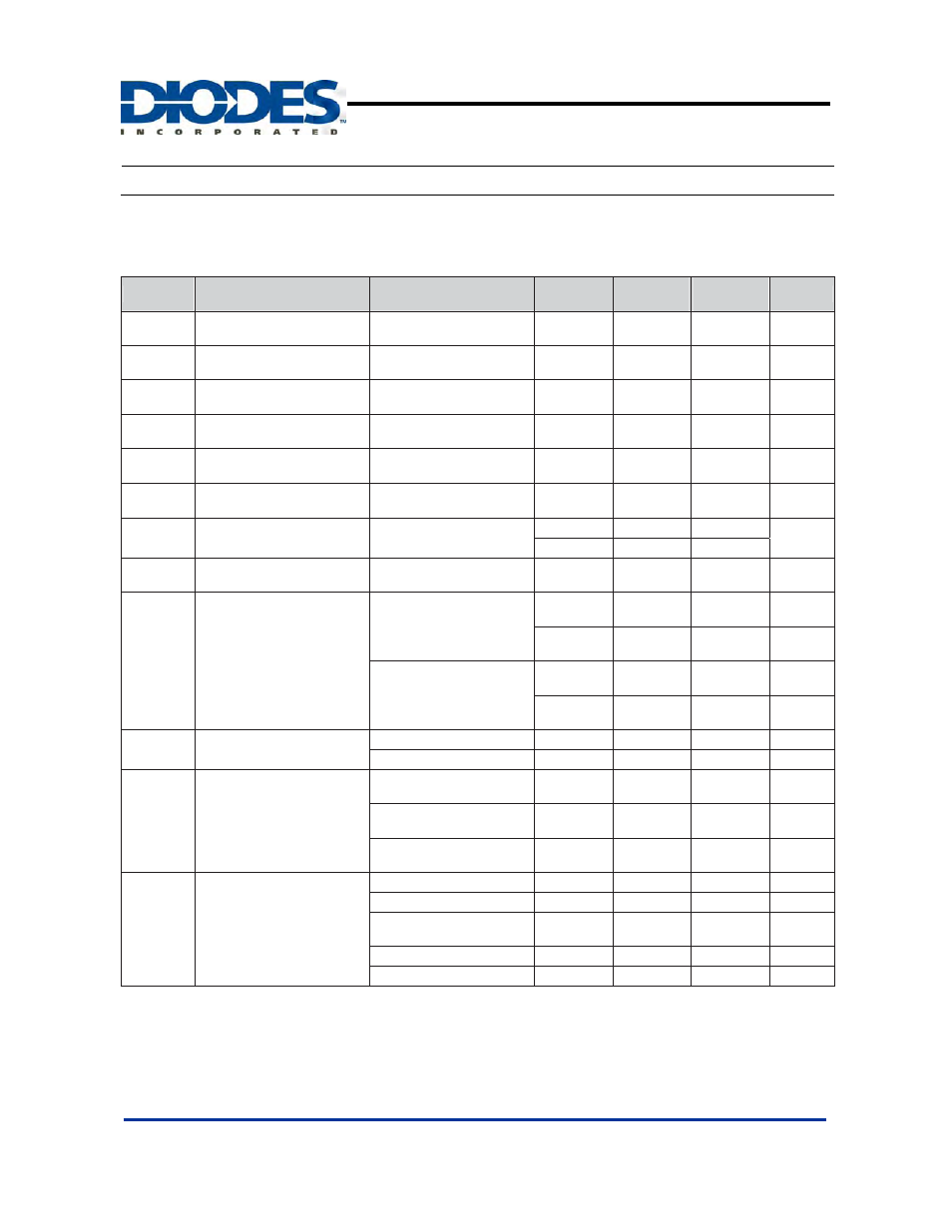
Electrical Characteristics
(Continued)
5V DC Electrical Characteristics
Unless otherwise specified, all limits guaranteed for T
A
= 25°C, V
+
= 5V, V
-
= 0V, V
CM
= 2.0V, V
O
= V
+
/2 and
R
L
> 1 M
Ω. Boldface limits apply at the temperature extremes.
Symbol
Parameter
Test Conditions
Min
(Note 10)
Typ.
(Note 9)
Max
(Note 10)
Unit
V
OS
Input
Offset
Voltage
1.7
7
9
mV
TCV
OS
Input Offset Voltage
Average Drift
5
µV/°C
I
B
Input Bias Current
15
250
500
nA
I
OS
Input
Offset
Current
5
50
150
nA
CMRR
Common Mode Rejection
Ratio
0V
≤ V
CM
≤ 4.7V
50 65 dB
PSRR
Power Supply Rejection
Ratio
2.7V
≤ V
+
≤ 5V
V
O
= 1V, V
CM
= 1V
50 60 dB
V
CMR
Input Common-Mode
Voltage Range
For CMRR
≥ 50dB
0 -0.2
V
4.8
A
V
Large Signal Voltage Gain R
L
= 2 k
Ω (Note 11)
15
10
100
V/mV
V
O
Output
Swing
R
L
= 2 k
Ω to 2.5V
V
+
- 300
V
+
- 400
V
+
- 50
mV
50
300
400
mV
R
L
= 10 k
Ω to 2.5V
V
+
- 100
V
+
- 200
V
+
- 10
mV
10
180
280
mV
I
O
Output Short Circuit
Current
Sourcing, V
O
= 0V
5
60
mA
Sinking, V
O
= 5V
10
90
mA
I
S
Supply
Current
APX321
Single amplifier
110
140
µA
APX358
Both amplifiers
190
340
600
µA
APX324
All four amplifiers
340
680
1100
µA
θ
JA
Thermal Resistance
Junction-to-Ambient
SOT353 (Note 12)
330
°C/W
SOT25 (Note 12)
250
°C/W
TSSOP-14L
(Note 12)
100
°C/W
MSOP-8L (Note 12)
203
°C/W
SOP-8L (Note 12)
150
°C/W