New prod uc t ah1889, Pin descriptions, Functional block diagram – Diodes AH1889 User Manual
Page 2: Absolute maximum ratings
AH1889
Document number: DS36256 Rev. 1 - 2
2 of 7
April 2013
© Diodes Incorporated
NEW PROD
UC
T
AH1889
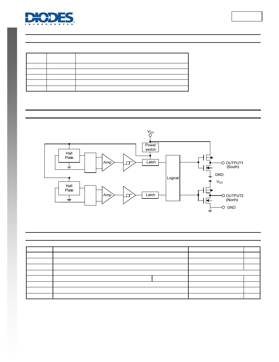
Pin Descriptions
Package: SOT553
Pin
Number
Pin
Name
Function
1
OUTPUT2
North Pole Setecting Output Pin (active low)
2 GND
Ground
3 NC
No Connection (Note 5)
4
V
DD
Power Supply Voltage
5
OUTPUT1
South Pole Detecting Output Pin (active low)
Note:
5. NC is “No Connection” pin and is not connected internally. This pin can be left open or tied to ground.
Functional Block Diagram
O
ffse
t
Can
cell
ing
Of
fs
et
Can
ce
lli
ng
Absolute Maximum Ratings
(Note 6) (@T
A
= +25°C, unless otherwise specified.)
Symbol Characteristics
Values
Unit
V
DD
Supply Voltage (Note 7)
5 V
V
DD_REV
Reverse Supply Voltage
-0.3 V
I
OUTPUT
Output current (source and sink)
1
mA
B
Magnetic Flux Density
Unlimited
P
D
Package Power Dissipation
SOT553
230
mW
Ts
Storage Temperature Range
-65 to +150
C
T
J
Maximum Junction Temperature
150
C
ESD
Human Body Model ESD capability
4
kV
Notes:
6. Stresses greater than the 'Absolute Maximum Ratings' specified above may cause permanent damage to the device. These are stress ratings only;
functional operation of the device at these or any other conditions exceeding those indicated in this specification is not implied. Device reliability may be
affected by exposure to absolute maximum rating conditions for extended periods of time.
7. The absolute maximum V
DD
of 6V is a transient stress rating and is not meant as a functional operating condition. It is not recommended to operate the
device at the absolute maximum rated conditions for any period of time.