Typical applications circuit, Pin descriptions, Am4961a – Diodes AM4961A User Manual
Page 2: A product line of diodes incorporated
AM4961A
Document number: DS36626 Rev. 1 - 2
2 of 17
October 2013
© Diodes Incorporated
AM4961A
A Product Line of
Diodes Incorporated
NE
W
P
R
OD
UC
T
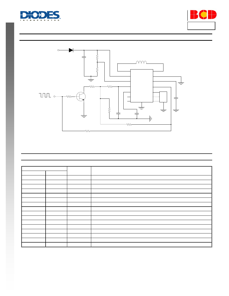
Typical Applications Circuit
OUT2
OUT1
VCC
GND
VMIN
CT
VPWM
VREF
COSC
HIN-
FG
HB
RD
HIN+
Hall
AM4961A
D1
C1
1
µF or greater
R1
27k
R2
10k
R4
39k
R6 330k
R7
100k
R5
100k
PWM
VCC
L1
R3 7.5k
R8
68k
C2
0.33
µF
C3
100pF
C4
0.47
µF
1 (1)
2 (3)
3 (4)
4 (5)
5 (6)
6 (7)
7 (8)
8 (9)
9 (10)
10 (11)
11 (12)
12 (13)
13 (14)
14 (15)
PGND
(16)
Q1
Typical Application Circuit with an External Input PWM Speed Control Signal
Note:
4. C1 is for power stabilization and should be 1µF or higher depending on the motor current and motor design.
Pin Descriptions
Package: HTSSOP-14 and SSOP16
Pin Number
Pin Name
Function
HTSSOP-14
SSOP-16
1
1
OUT2
Drive output 2
–
2
NC
No connection
2
3
VCC
Power supply
3
4
VMIN
Minimum duty setting
4
5
VPWM
Adjustable input
5
6
COSC
Oscillator capacitor
6
7
FG
Rotation speed indicator
7
8
RD
Rotation/lock state indicator
8
9
HIN+
Hall sensor input+
9
10
HB
Hall sensor bias regulator
10
11
HIN-
Hall sensor input-
11
12
VREF
Reference voltage regulator
12
13
CT
Lock and rotation setting capacitor terminal
13
14
GND
Ground for control circuit
14
15
OUT1
Drive output 1
–
16
PGND
Power ground