Data sheet – Diodes AM4961 User Manual
Page 11
Data Sheet
11
May. 2011 Rev. 2. 4
BCD Semiconductor Manufacturing Limited
SINGLE PHASE FULL WAVE DIRECT PWM MOTOR DRIVER AM4961
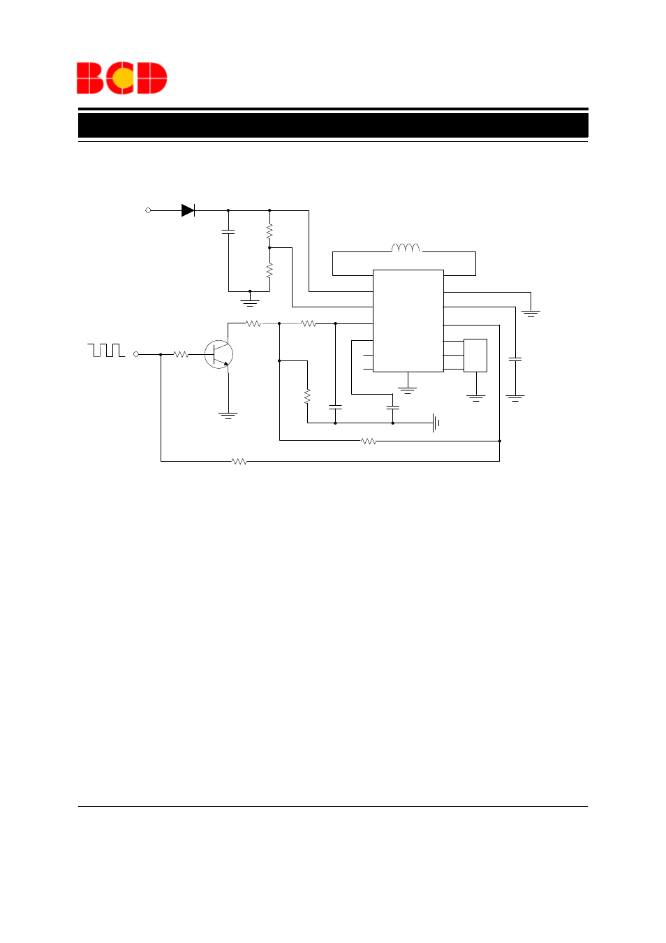
Typical Application
Figure 11. Typical Application of AM4961 (Note 6)
Note 6:
*1. Ground Line Layout
PGND is connected to motor supply stage and GND is
connected to control stage. All ground lines from control
stage are connected to GND.
*2. Stability of Power Supply
C1 is employed to stabilize V
CC
. Its capacitance is no less
than 1
μF.
*3. Hall Input
To avoid noise, the shortest line is recommended to con-
nect with Hall stage which has about 20mV hysteresis.
Thus, the ideal Hall input is 50mV or over.
*4. COSC Capacitor
When C
CP
is 100pF, the COSC frequency will be 25kHz.
*5. FG Output
FG output terminal is open collector output which varies
with phase change.
*6. RD Output
RD output terminal is open collector output. It is low at
rotation mode and high when stopped.
*7. HB Pin
This pin is available to output a 1.25V Hall bias voltage.
*8. VMIN Pin
If this pin is disused, connect it directly with VPWM, the
minimum duty cycle will be 10%.
OUT2
OUT1
VCC
GND
VMIN
CT
VPWM
VREF
COSC
HIN-
FG
HB
RD
HIN+
Hall
AM4961
D1
C1
1
μF or greater
R1
27k
R2
10k
R4
39k
R6 330k
R7
100k
R5
100k
PWM
VCC
L1
R3 7.5k
R8
68k
C2
0.33
μF
C3
100pF
C4
0.47
μF
1 (1)
2 (3)
3 (4)
4 (5)
5 (6)
6 (7)
7 (8)
8 (9)
9 (10)
10 (11)
11 (12)
12 (13)
13 (14)
14 (15)
PGND
(16)