Data sheet, Application information (continued) – Diodes AM9789 User Manual
Page 13
Data Sheet
Single Phase Full-wave Motor Driver for Silent Fan Motor AM9789
Oct. 2012 Rev. 1. 1 BCD Semiconductor Manufacturing Limited
13
Application Information
(Continued)
operated with the PWM pin open, the built-in resistor
enables the PWM pin to change to high-level voltage
and the motor speed rises to full speed. When the
PWM pin is fixed at low-level voltage, the motor
decelerates, and after the motor stops, it enters
“Power Saving Mode”. Figure 12 shows a rotating
fan’s waveform at PWM Mode. Figure 13 shows
Lock Mode Waveform at PWM input condition in the
same fan.
Figure 12. PWM Mode Waveform
(
PWM: 50% duty cycle, V
H
=5V, V
L
=0V)
Figure 13. Lock Mode at PWM Input Condition
(
PWM: 50% duty cycle, V
H
=5V, V
L
=0V)
9. Frequency Generator Function
The FG pin is an open collector output, connecting a
pull-up resistor to a high level voltage for the
frequency generator function. During the lock mode,
FG pin output will be always high. Open the terminal
when not in use. Figure 14 shows how this function
works.
Figure 14. Rotation Mode Waveform
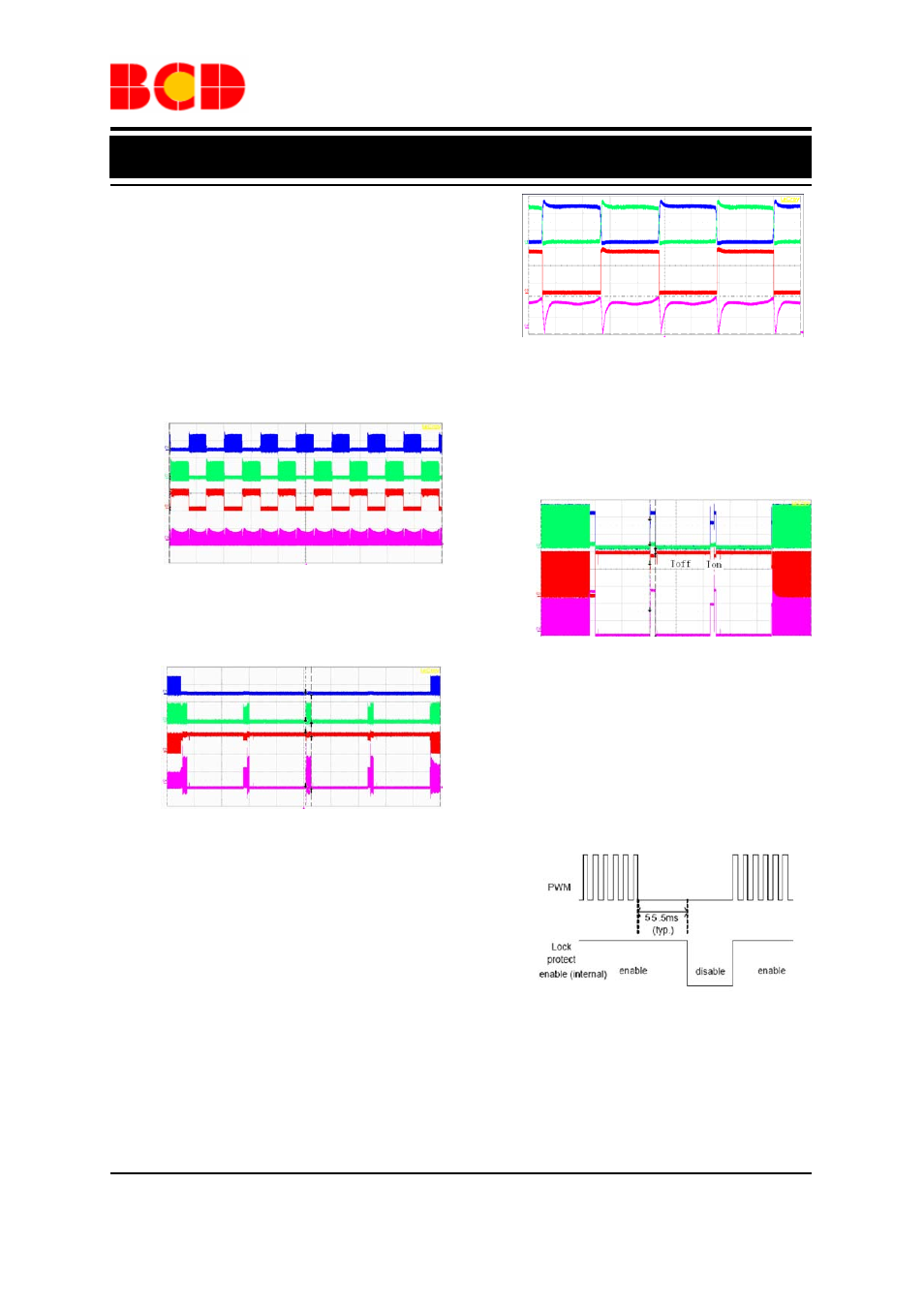
10. Lock Protection and Auto-restart
The IC detects the rotation of the motor by Hall
signal and the lock detection ON time (t
ON
) and OFF
time (t
OFF
) are adjusted by the internal counter. As
showed below.
Figure 15. Lock Mode Waveform
11. Quick Start and Standby Mode
The IC will enter standby mode when PWM input
keeps low level for more than 55ms (typ.). In standby
mode, shutdown amplifier and FG will be shutdown,
and the supply current is around 130
µA. In standby
mode, the lock protection function doesn’t work; the
fan will restart when released from standby mode.
Figure 16 describes this function.
Figure 16. Quick Start and Standby Mode
Time 2s/div
V
OUT1
5V/div
V
OUT2
5V/div
V
FG
5V/div
I
IN
200mA/div
V
OUT2
2V/div
V
FG
2V/div
I
IN
200mA/div
V
OUT1
2V/div
V
OUT2
2V/div
V
FG
2V/div
I
IN
200mA/div
Time 2ms/div
Time 2s/div
Time 10ms/div
V
OUT1
5V/div
V
OUT2
5V/div
V
FG
5V/div
I
IN
200mA/div
V
OUT1
2V/div