Data sheet, Pin description – Diodes AP3041 User Manual
Page 3
Data Sheet
Boost Controller for WLED Driver in Medium-sized LCD Panel AP3041
Oct. 2012 Rev. 1. 2 BCD Semiconductor Manufacturing Limited
3
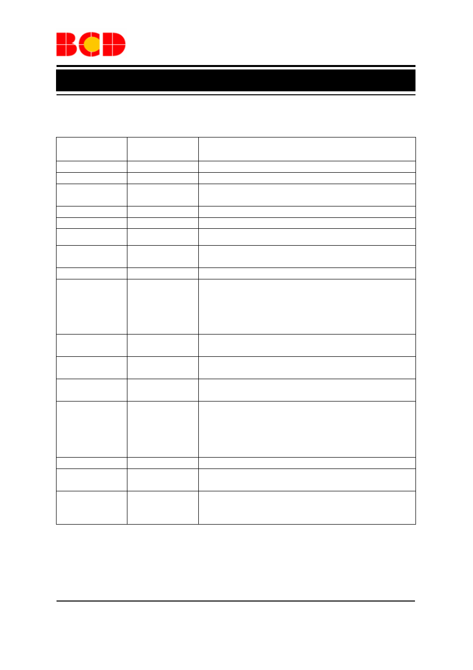
Pin Description
Pin Number
Pin Name
Function
1
CT
Capacitor setting shut down delay time
2
OV
Over output voltage protection pin
3 UVLO
Two resistors connected from this pin to GND and the power
supply respectively are used to set start-up and shutdown level
4 EN
Enable
pin
5
VIN
Input supply pin. This pin must be locally bypassed
6
VCC
This pin should be bypassed to GND with a ceramic capacitor
7 OUT
Connect this pin to the gate of external MOSFET, the gate driver
has 1A peak current capability
8 GND
Ground
9 FAULT
This pin can be used to drive the external MOSFET. The logic of
the driver signal is controlled by that of
PWM
pin and the signal
phase of them is the same. This pin is pulled to ground under fault
condition of OVP, UVLO, OTP, diode short circuit and LED
short circuit.
10 RT
An external resistor connected from this pin to GND is used to set
the operating frequency
11 CS
Sense switch current pin, which is used for current mode control
and for current limit. The current limit voltage is 500mV
12 SC
Slope compensation for current sense. A resistor between SC and
GND will program the slope compensation
13 SS/COMP
An external soft-start time capacitor is placed from this pin to
GND and is charged by an internal 20
μA current source to control
regulator soft-start time.
Compensation pin. This pin is the output of the internal error
amplifier.
14
FB
Voltage feedback pin. The reference voltage is 500mV
15 PWM
This pin can be connected to current matched chip and receives
error signal used to shut down the system
16 FLAG
Fault condition output pin. When the output is in short circuit
condition, the FLAG outputs logic low to shut down the power
path. Please refer to the application circuit