Recommended operating conditions, Electrical characteristics, Ap8803 – Diodes AP8803 User Manual
Page 3
AP8803
Document number: DS31970 Rev. 5 - 2
3 of 10
August 2012
© Diodes Incorporated
AP8803
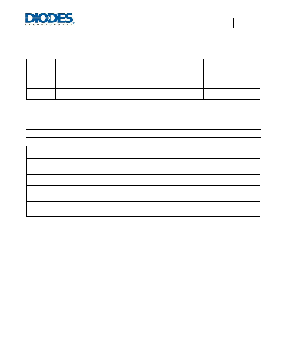
Recommended Operating Conditions
(@T
A
= +25°C, unless otherwise specified.)
Symbol Parameter Min
Max
Unit
V
IN
Operating
Input
Voltage
8.0
30
V
V
CTRLH
Voltage
High
0.3
2.5
V
V
CTRLL
Voltage
Low
0.25
V
I
SW
Continuous Switch Current (Note 5)
1
A
T
A
Ambient Temperature Range
-40
+125
°C
Duty Cycle
Using Inductor
≥ 100µH (Note 4)
0.1
0.95
Notes:
4. For most applications the LED current will be within 8% over the duty cycle range specified. Duty cycle accuracy is also dependent on
propagation delay. Smaller size inductors can be used but LED current accuracy may be greater than 8% at extremes of duty cycle. This is
most noticeable at low duty cycles (less than 0.1) or when the input voltage is high and only one LED is being driven.
5. Refer to Figure 8 for the device derating curve.
Electrical Characteristics
(@T
A
= +25°C, unless otherwise specified.)
Symbol Parameter
Conditions Min
Typ
Max
Unit
V
INSU
Internal Regulator Start-Up Threshold
V
IN
rising
5.65 V
V
INSD
Internal Regulator Shutdown Threshold V
IN
falling
5.55 V
I
Q
Quiescent Current
CTRL pin floating f = 250kHz
1.8
5
mA
V
THD
Internal Threshold Voltage
92
100
108
mV
I
SET
SET Pin Input Current
V
SET
= V
IN
-0.1
1.25
10
µA
V
REF
Internal Reference Voltage
1.25
V
R
DS(on)
On Resistance of MOSFET
I
SW
= 1A
0.5
1
Ω
I
SW
Continuous Switch Current
(Note 5)
1
A
I
SW_Leakage
Switch
Leakage
Current
8
µA
f
OSC
Switching
Frequency
0.7 MHz
θ
JA
Thermal Resistance Junction-to-
Ambient
TSOT25 (Note 6)
125
°C/W
Notes:
5. Refer to Figure 8 for the device derating curve.
6. Test condition for TSOT25: Device mounted on FR-4 PCB, 25mm x 25mm, 2oz copper, minimum recommended pad layout on top layer and
thermal vias to bottom layer ground plane. For better thermal performance, larger copper pad for heat-sink is needed.