Al8811, Absolute maximum ratings, Recommended operating conditions – Diodes AL8811 User Manual
Page 3: Electrical characteristics
AL8811
Document number: DS36090 Rev. 2 - 2
3 of 11
June 2013
© Diodes Incorporated
AL8811
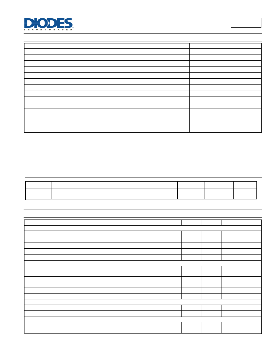
Absolute Maximum Ratings
(@T
A
= +25°C, unless otherwise specified.)
Symbol Parameter
Rating
Unit
V
CC
Power Supply Voltage
20
V
V
IR
Comparator Input Voltage Range
-0.3 to +36
V
V
C (SWITCH)
“Current Switch +” Collector Voltage
36
V
V
E (SWITCH)
„Current Switch –„ Emitter Voltage (V
PIN
1 = 36V)
36 V
V
CE (SWITCH)
“Current Switch” Collector to Emitter Voltage
36
V
V
C (DRIVER)
“Current Drive” Collector Voltage
36
V
I
C (DRIVER)
“Current Drive” Collector Current
100
mA
I
SW
“Current Switch” Current
1.6
A
P
D
Power Dissipation (Note 4)
600
mW
JA
Thermal Resistance
130
C/W
T
MJ
Maximum Junction Temperature
+150
C
T
STG
Storage Temperature Range
-65 to +150
C
ESD HBM
Human Body Model ESD Protection
1
kV
ESD MM
Machine Model ESD Protection
150
V
Caution:
Stresses greater than the 'Absolute Maximum Ratings' specified above, may cause permanent damage to the device. These are stress ratings only;
functional operation of the device at these or any other conditions exceeding those indicated in this specification is not implied. Device reliability may be
affected by exposure to absolute maximum rating conditions for extended periods of time.
Semiconductor devices are ESD sensitive and may be damaged by exposure to ESD events. Suitable ESD precautions should be taken when handling
and transporting these devices.
Recommended Operating Conditions
Symbol
Parameter
Min
Max
Unit
V
CC
Supply Voltage
3
20
V
T
OP
Operating Junction Temperature Range
-40
+105
C
Electrical Characteristics
(@ V
CC
= 5V, T
A
= +25°C, unless otherwise specified.)
Symbol Parameter Min
Typ
Max
Unit
OSCILLATOR
f
OSC
Frequency
(V
PIN
5 = 0V, C
T
= 1.0nF, T
A
= +25°C)
24 33 42 kHz
I
CHG
Charge
Current
(V
CC
= 5.0V to 20V, T
A
= +25°C)
24 30 42 µA
I
DISCHG
Discharge Current (V
CC
= 5.0V to 20V, T
A
= +25°C)
140 200 260 µA
I
DISCHG
/ I
CHG
Discharge to Charge Current Ratio (Pin 7 to V
CC
, T
A
= +25°C)
5.2 6.5 7.5 —
V
IPK (SENSE)
Current Limit Sense Voltage (I
CHG
= I
DISCHG
, T
A
= +25°C)
300 400 450 mV
OUTPUT SWITCH (Note 4)
V
CE(sat)
Saturation Voltage, Darlington Connection
(I
SW
= 1.0A, Pins 1, 8 connected)
— 1.0 1.3 V
V
CE(sat)
Saturation Voltage, Darlington Connection
(I
SW
= 1.0A, ID = 50mA, Forced ß 20)
— 0.45 0.7 V
h
FE
DC Current Gain (I
SW
= 1.0A, V
CE
= 5.0V, T
A
= +25°C)
50 75 —
—
I
C(off)
Collector Off-State Current (V
CE
= 20V)
— 0.01 100 µA
COMPARATOR
V
th
Threshold Voltage T
A
= +25°C
1.225
1.25
1.275
V
Reg
(LINE)
Threshold Voltage Line Regulation (V
CC
= 3.0V to 20V)
— 1.4 6.0 mV
TOTAL DEVICE
I
CC
Supply Current (V
CC
= 5.0V to 20V, C
T
=1.0nF, Pin 7 = V
CC
,
V
PIN 5
> V
th
Pin 2 = Gnd, remaining pins open)
—
—
3.5 mA