Recommended operating conditions, Electrical characteristics, Al8807q – Diodes AL8807Q User Manual
Page 3
AL8807Q
Document number: DS36904 Rev. 1 - 2
3 of 16
March 2014
© Diodes Incorporated
AL8807Q
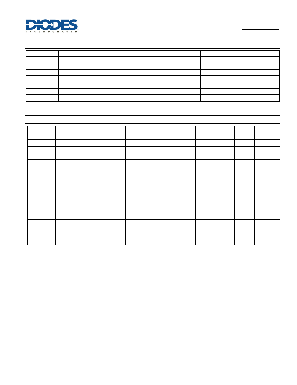
Recommended Operating Conditions
(@T
A
= +25°C, unless otherwise specified.)
Symbol
Parameter
Min
Max
Unit
V
IN
Operating Input Voltage relative to GND
6.0
30
V
V
CTRLH
Voltage High for PWM dimming relative to GND
2.6
5.5
V
V
CTRLDC
Voltage range for 20% to 100% DC dimming relative to GND
0.5
2.5
V
V
CTRLL
Voltage Low for PWM dimming relative to GND
0
0.4
V
f
SW
Maximum switching frequency
—
1
MHz
I
SW
Continuous switch current
—
1.3
A
T
J
Junction Temperature Range
-40
125
°C
Electrical Characteristics
(@ V
IN
= 12V, T
A
= +25°C, unless otherwise specified.)
Symbol Parameter
Conditions Min
Typ
Max
Unit
V
INSU
Internal regulator start up threshold
V
IN
rising
— — 5.9 V
V
INSH
Internal regulator hysteresis threshold V
IN
falling
100 — 300 mV
I
Q
Quiescent current
Output not switching (Note 5)
—
—
350
µA
I
S
Input supply Current
CTRL pin floating f = 250kHz
—
1.8
5
mA
V
TH
Set current Threshold Voltage
—
95
100
105
mV
V
TH-H
Set threshold hysteresis
—
—
±20
—
mV
I
SET
SET pin input current
V
SET
= V
IN
-0.1
— 16 22 µA
R
CTRL
CTRL pin input resistance
Referred to internal reference
—
50
—
kΩ
V
REF
Internal Reference Voltage
—
—
2.5
—
V
R
DS(on)
On Resistance of SW MOSFET
I
SW
= 1A
— 0.25 0.4
Ω
t
R
SW rise time
V
SENSE
= 100±20mV, f
SW
= 250kHz
V
SW
= 0.1V~12V~0.1V C
L
= 15pF
— 12 — ns
t
F
SW fall time
— 20 — ns
I
SW_Leakage
Switch leakage current
V
IN
=30V
— — 0.5 μA
JA
Thermal Resistance Junction-to-
Ambient (Note 6)
(Note 7)
—
69
—
C/W
JC
Thermal Resistance Junction-to-case
(Note 8)
(Note
7)
— 4.3 — —
Notes:
5. AL8807Q does not have a low power standby mode but current consumption is reduced when output switch is inhibited: V
SENSE
= 0V. Parameter is
tested with V
CTRL
≤ 2.5V
6. Refer to figure 35 for the device derating curve.
7. Test condition for MSOP-8EP: Device mounted on FR-4 PCB (51mm x 51mm 2oz copper, minimum recommended pad layout on top layer and
thermal vias to bottom layer with maximum area ground plane. For better thermal performance, larger copper pad for heat-sink is needed
8. Dominant conduction path via exposed pad.