Al8807q, Pin descriptions, Functional block diagram – Diodes AL8807Q User Manual
Page 2: Absolute maximum ratings
AL8807Q
Document number: DS36904 Rev. 1 - 2
2 of 16
March 2014
© Diodes Incorporated
AL8807Q
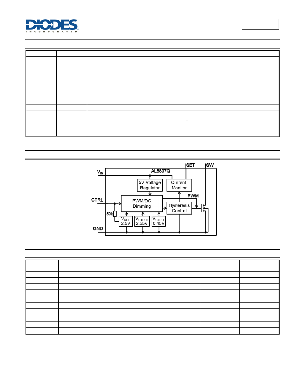
Pin Descriptions
Pin Name
Pin Number
Functions
SET
1
Set Nominal Output Current Pin. Configure the output current of the device.
GND
2, 3
GND Pin
CTRL
4
Dimming and On/Off Control Input.
Leave floating for normal operation.
(V
CTRL
= V
REF
= 2.5V giving nominal average output current I
OUTnom
= 0.1/R
S
)
Drive to voltage below 0.4V to turn off output current
Drive with DC voltage (0.5V < V
CTRL
< 2.5V) to adjust output current from 20% to 100% of I
OUTnom
A PWM signal (low level ≤ 0.4V and high level > 2.6; transition times less than 1us) allows the output
current to be adjusted below the level set by the resistor connected to SET input pin.
SW
5, 6
Switch Pin. Connect inductor/freewheeling diode here, minimizing track length at this pin to reduce EMI.
N/C 7
no
connection
V
IN
8
Input Supply Pin. Must be locally decoupled to GND with > 2.2µF X7R ceramic capacitor – see applications
section for more information.
EP EP
Exposed pad/TAB connect to GND and thermal mass for enhanced thermal impedance. Should not be used as
electrical ground conduction path.
Functional Block Diagram
Absolute Maximum Ratings
(@T
A
= +25°C, unless otherwise specified.)
Symbol Parameter Ratings
Unit
ESD HBM
Human Body Model ESD Protection
4000
V
ESD MM
Machine Model ESD Protection
300
V
ESD CDM
Charged Device Model ESD Protection
1000
V
V
IN
Continuous V
IN
pin voltage relative to GND
-0.3 to +40
V
V
SW
SW voltage relative to GND
-0.3 to +40
V
V
CTRL
CTRL pin input voltage
-0.3 to +6
V
I
SW-RMS
DC or RMS Switch current
1.6
A
I
SW-PK
Peak Switch current (<10%)
2.5
A
T
J
Junction Temperature
+150
°C
T
LEAD
Lead Temperature Soldering
+300
°C
T
ST
Storage Temperature Range
-65 to +150
°C
Caution: Stresses greater than the 'Absolute Maximum Ratings' specified above, may cause permanent damage to the device. These are stress ratings only;
functional operation of the device at these or any other conditions exceeding those indicated in this specification is not implied. Device reliability may be
affected by exposure to absolute maximum rating conditions for extended periods of time.
Semiconductor devices are ESD sensitive and may be damaged by exposure to ESD events. Suitable ESD precautions should be taken when handling
and transporting these devices.