Al8807, Application information – Diodes AL8807 User Manual
Page 14
AL8807
Document number: DS35281 Rev. 5 - 2
14 of 20
March 2013
© Diodes Incorporated
AL8807
Application Information
(cont.)
EMI and Layout Considerations
The AL8807 is a switching regulator with fast edges and measures small differential voltages; as a result of this care has to be taken with
decoupling and layout of the PCB.To help with these effects the AL8807 has been developed to minimise radiated emissions by controlling the
switching speeds of the internal power MOSFET. The rise and fall times are controlled to get the right compromise between power dissipation due
to switching losses and radiated EMI. The turn-on edge (falling edge) dominates the radiated EMI which is due to an interaction between the
Schottky diode (D1), Switching MOSFET and PCB tracks. After the Schottky diode reverse recovery time of around 5ns has occurred; the falling
edge of the SW pin sees a resonant loop between the Schottky diode capacitance and the track inductance, L
TRACK
, See figure 36.
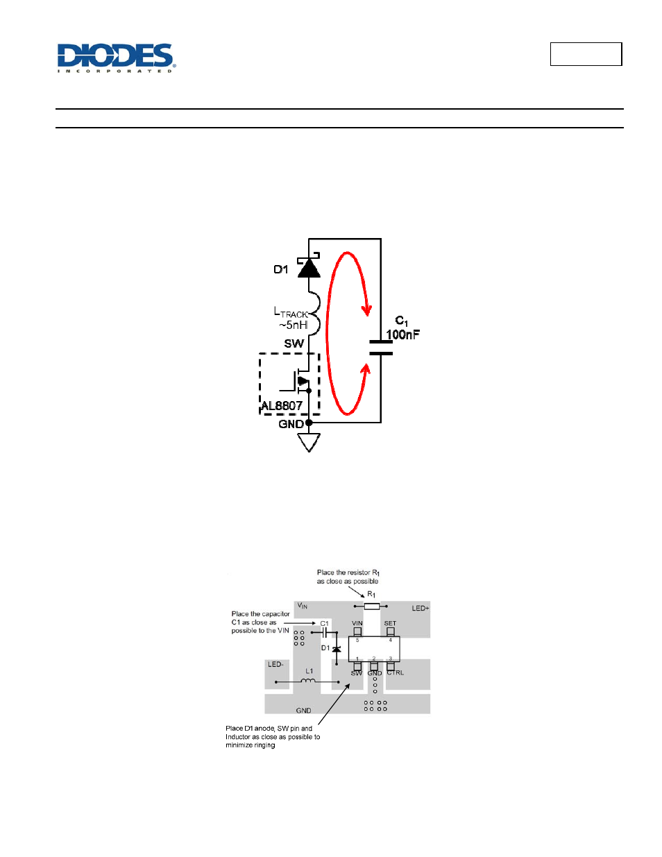
Figure 36 PCB Loop Resonance
The tracks from the SW pin to the Anode of the Schottky diode, D1, and then from D1’s cathode to the decoupling capacitors C1 should be as short
as possible. There is an inductance internally in the AL8807 this can be assumed to be around 1nH. For PCB tracks a figure of 0.5nH per mm can
be used to estimate the primary resonant frequency. If the track is capable of handling 1A increasing the thickness will have a minor effect on the
inductance and length will dominate the size of the inductance. The resonant frequency of any oscillation is determined by the combined
inductance in the track and the effective capacitance of the Schottky diode. An example of good layout is shown in figure 37 - the stray track
inductance should be less than 5nH.
Figure 37 Recommended PCB Layout