Al8806q, Recommended operating conditions, Electrical characteristics – Diodes AL8806Q User Manual
Page 3
AL8806Q
Document number: DS36905 Rev. 1 - 2
3 of 13
www.diodes.com
April 2014
© Diodes Incorporated
AL8806Q
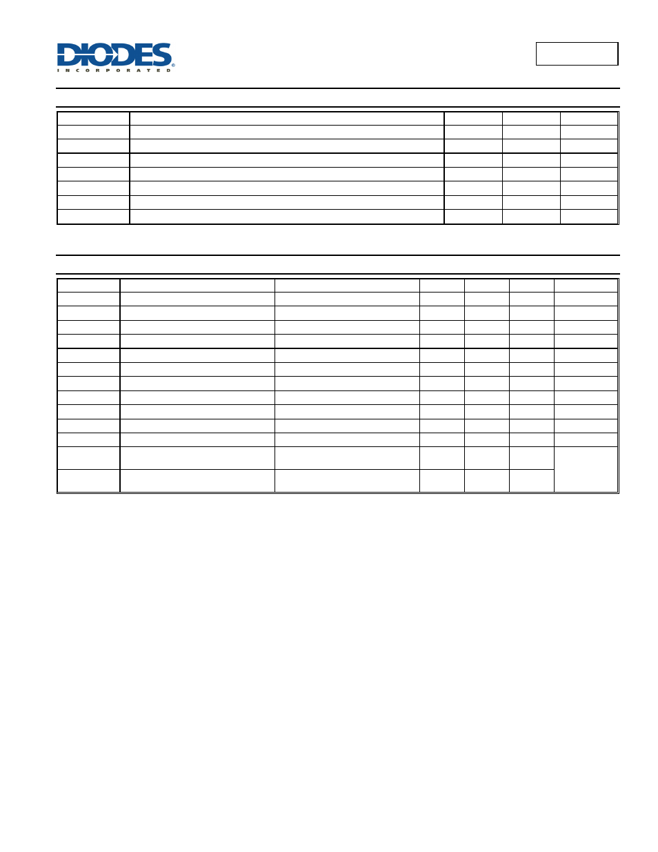
Recommended Operating Conditions
(@T
A
= +25°C, unless otherwise specified.)
Symbol
Parameter
Min
Max
Unit
V
IN
Operating Input Voltage relative to GND
6.0
30
V
V
CTRLH
Voltage High for PWM Dimming Relative to GND
2.6
5.5
V
V
CTRLDC
Voltage range for 20% to 100% DC Dimming Relative to GND
0.5
2.5
V
V
CTRLL
Voltage Low for PWM Dimming Relative to GND
0
0.4
V
f
SW
Maximum Switching Frequency
—
1
MHz
I
SW
Continuous Switch Current
—
1.5
A
T
J
Junction Temperature Range
-40
+125
°C
Electrical Characteristics
(@ V
IN
= 12V, T
A
= +25°C, unless otherwise specified.)
Symbol Parameter
Conditions
Min
Typ.
Max
Unit
V
INSU
Internal regulator start up threshold
V
IN
rising
—
—
5.9 V
V
INSH
Internal regulator hysteresis threshold V
IN
falling
100
—
300 mV
I
Q
Quiescent current
Output not switching
(Note 5)
—
— 350 µA
I
S
Input supply Current
CTRL pin floating f = 250kHz
—
1.8 5 mA
V
TH
Set current Threshold Voltage
V
CTRL
≥ 2.6V or floating.
95 100 105 mV
V
TH-H
Set threshold hysteresis
—
—
±20
—
mV
I
SET
SET pin input current
V
SET
= V
IN
-0.1
— 16 22 µA
R
CTRL
CTRL pin input resistance
Referred to internal reference
—
50
—
kΩ
V
REF
Internal Reference Voltage
—
—
2.5
—
V
R
DS(on)
On Resistance of SW MOSFET
I
SW
= 1A
— 0.18 0.35
Ω
I
SW_Leakage
Switch leakage current
V
IN
= 30V
— — 0.5 μA
θ
JA
Thermal Resistance Junction-to-
Ambient (Note 6)
(Note 7)
—
69
—
°C/W
θ
JC
Thermal Resistance Junction-to-Case
(Note 6)
(Note
7)
— 4.3 —
Notes: 5. AL8806Q does not have a low power standby mode but current consumption is reduced when output switch is inhibited: V
SENSE
= 0V. Parameter is tested
with V
CTRL
≤ 2.5V
6. Refer to figure 5 for the device derating curve.
7. Measured on an FR4 51x51mm PCB with 2oz copper standing in still air with minimum recommended pad layout on top layer and thermal vias to bottom
layer maximum area ground plane. For better thermal performance, larger copper pad for heat-sink is needed.
8. Dominant conduction path via exposed pad. Refer to figure 5 for the device derating curve.