Ap5724, Pin descriptions, Functional block diagram – Diodes AP5724 User Manual
Page 2: Absolute maximum ratings
AP5724
Document number: DS31843 Rev. 4 - 2
2 of 15
December 2013
© Diodes Incorporated
AP5724
Pin Descriptions
Pin Name
Functions
SW
Switch Pin. Connect inductor/diode here. Minimize trace area at this pin to reduce EMI.
GND GND
pin.
FB
Feedback Pin. Reference voltage is 0.1V. Connect cathode of lowest LED and a sense resister here. Calculate resistor value
according to the formula: R
SET
= 0.1V / ILED
EN
Converter On/Off Control Input. A high input at EN turns the converter On, and a low input turns it off. If On/Off control is not
needed, connect EN to the input source for automatic startup. The EN pin cannot be left floating.
OVP
Output Voltage detect pin for over voltage protection.
V
IN
Input Supply Pin. Must be locally bypassed with 1μF or 2.2μF to reduce input noise.
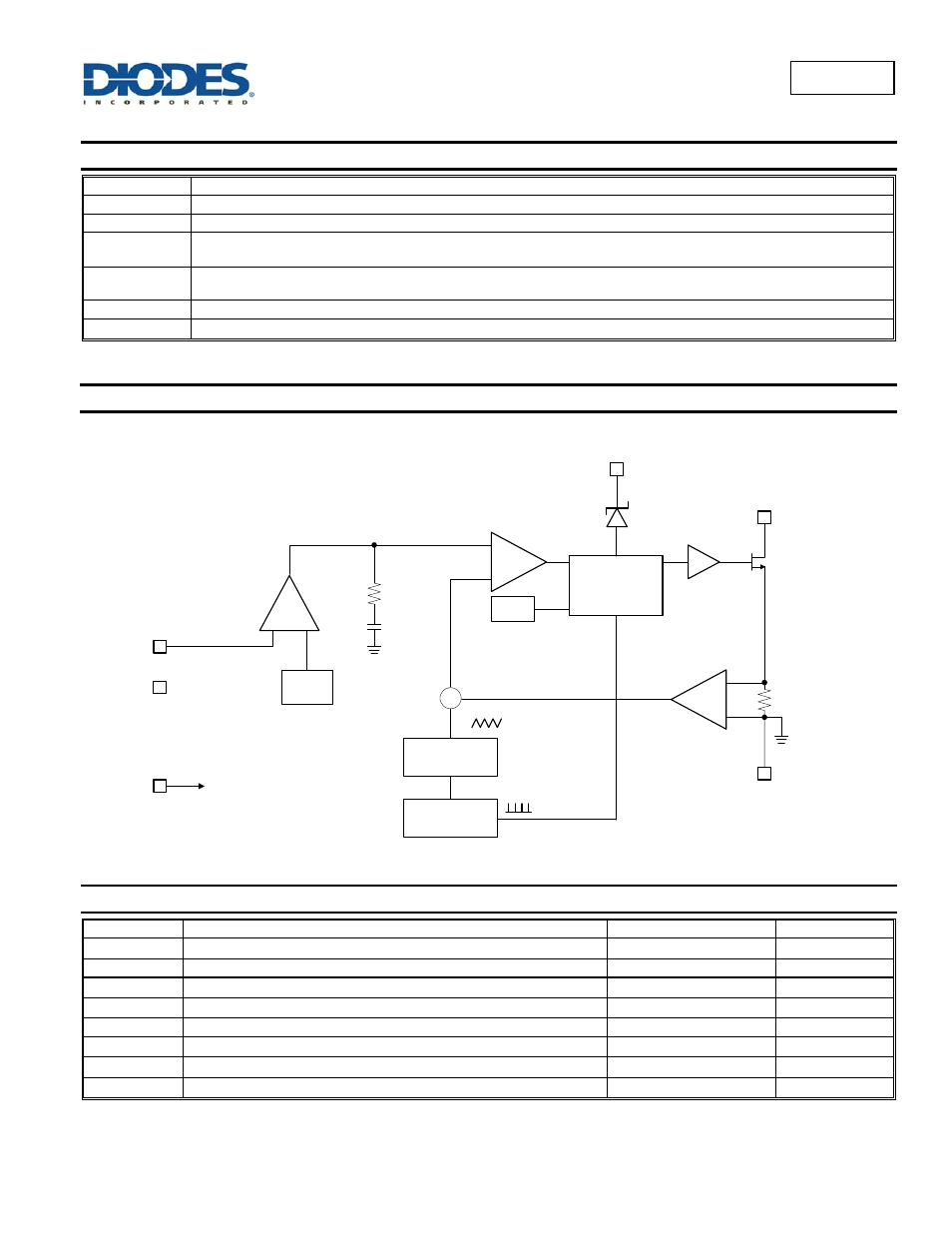
Functional Block Diagram
1.2MHz
Oscillator
RAMP
Generator
Σ
-
+
-
+
-
+
V
REF
0.1V
VIN
3
FB
Rc
Cc
Comparator
A2
CONTROL
LOGIC
A1
1
Driver
SW
Q1
2 GND
4
EN
Enable
6
OTP
5
OVP
Absolute Maximum Ratings
(@T
A
= +25°C, unless otherwise specified.)
Symbol Parameter
Rating
Unit
V
IN
VIN Pin Voltage
-0.3 to +7
V
VSW
SW Voltage
-0.3 to +34
V
V
OVP
OVP Pin Voltage
-0.3 to +35
V
V
FB
Feedback Pin Voltage
-0.3 to +7
V
EN EN
-0.3 to +7
V
T
J(MAX)
Maximum Junction Temperature
150
°C
T
LEAD
Lead Temperature
300
°C
T
ST
Storage Temperature Range
-65 to +150
°C
Caution:
Operation above the absolute maximum ratings can cause device failure. These values, therefore, must not be exceeded under any condition.
Operation at the absolute maximum rating for extended periods, may reduce device reliability.