Al3159, New prod uc t absolute maximum ratings, Recommended operating conditions – Diodes AL3159 User Manual
Page 3: Electrical characteristics
AL3159
HIGH EFFICIENCY 1x/2x CHARGE PUMP
FOR WHITE LED APPLICATIONS
AL3159
Document number: DS35048 Rev. 2 - 2
3 of 10
January 2011
© Diodes Incorporated
NEW PROD
UC
T
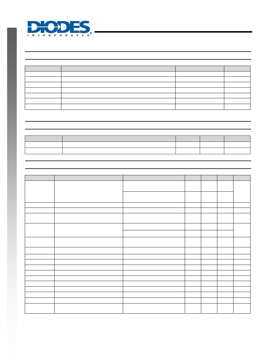
Absolute Maximum Ratings
(Note 2)
Symbol
Description
Rating
Unit
ESD HBM
Human Body Model ESD Protection
2
KV
ESD MM
Machine Model ESD Protection
200
V
V
IN
Input Voltage
-0.3 to 6
V
V
CTL1,2,3
CTL1, CTL2, CTL3 to GND Voltage
-0.3 to V
IN
+0.3
V
I
OUT
Maximum DC Output Current
270
mA
T
J
Operating Junction Temperature Range
150
°C
T
LEAD
Maximum Soldering Temperature (at leads, 10 sec)
300
°C
Notes: 2. Exceeding Absolute Maximum Ratings will cause permanent damage to the device.
Recommended Operating Conditions
Symbol
Parameter
Min
Max
Unit
V
IN
Input
Voltage
2.7 5.5
V
T
A
Operating Ambient Temperature
-40
85
°C
Electrical Characteristics
(T
A
= 25
°C, V
IN
= 3.6V, C
IN
= C
OUT
= 2.2µF, C
1
= 1µF Unless otherwise noted)
Symbol
Parameter
Test Conditions
Min
Typ.
Max
Unit
I
Q
Quiescent
Current
1x Mode, 3.0≤V
IN
≤5.5, Active,
No Load Current
0.3
0.6
mA
2x Mode, 3.0≤V
IN
≤5.5, Active,
No Load Current
2 5
I
SHDN
Shutdown Current
CTL1, CTL2 and CTL3 = 0
1
µA
I
DX
I
SINK
Current Accuracy (Note 3)
19 20 21 mA
I
D-Match
Current Matching Between Any Two
Current Sink Inputs (Note 4)
V
F
: D1:D9 = 3.6V
1
2
%
R
out
Open Loop V
OUT
Resistance
1x mode
0.5
Ω
2 x mode
4.5
V
TH
1x to 2x Transition Threshold at Any
I
SINK
Pin
I
DX
= 20mA
150
mV
V
HS
Mode Transition Hysteresis
250
mV
T
SS
Soft-Start
Time
100 µs
Fsw Switching
Frequency
1.2 MHz
V
CTL1, 2,3 (L)
CTL1,2,3
Threshold
Low
V
IN
= 2.7V
0.4
V
V
CTL1,2,3(H)
CTL1,2,3
Threshold
High
V
IN
= 5.5V
1.4
V
T
CTL1,2,3
CTL1,2,3
Off
Timeout
200 µs
UVLO V
IN
Under-Voltage Lockout
1.8
2
2.2
V
I
CTL1,2,3
CTL1,2,3 Input Leakage
-1
1
µA
T
SHDN
Thermal shutdown Protection
160
°C
T
HYS
Thermal shutdown hysteresis
10
°C
θ
JA
Thermal Resistance Junction-to-
Ambient
QFN3030-20 (Note 5)
48
o
C/W
Notes: 3. Determined by the average current levels of all active channels
4. Defined as the deviation of any sink current from the average of all active current channels.
5. Device mounted on FR-4 substrate, 2"*2", 2oz copper, double-sided PC board, with minimum recommended pad on top layer and
4 vias to bottom layer.