Al3159, New prod uc t pin descriptions, Functional block diagram – Diodes AL3159 User Manual
Page 2
AL3159
HIGH EFFICIENCY 1x/2x CHARGE PUMP
FOR WHITE LED APPLICATIONS
AL3159
Document number: DS35048 Rev. 2 - 2
2 of 10
January 2011
© Diodes Incorporated
NEW PROD
UC
T
Pin Descriptions
Pin Name
Pin Number
Description
D8
1
Current sink input #8. Connected to V
OUT
when un-used.
D9
2
Current sink input #9. Connected to V
OUT
when un-used.
CTL1
3
Control Pin 1
CTL3
4
Control Pin 3
CTL2
5
Control Pin 2
PGND
6
Charge Pump Switch Ground
CN
7
Negative Terminal of Flying Capacitor
V
IN
8
Input Power Supply. Requires 2.2µF capacitor between this pin and ground.
CP
9
Positive Terminal of Flying Capacitor
NC 10,19
No-Connect
V
OUT
11
Charge pump output to drive load circuit. Requires 2.2µF capacitor between this pin
and ground.
D1
12
Current sink input #1. Connected to V
OUT
when un-used.
D2
13
Current sink input #2. Connected to V
OUT
when un-used.
D3
14
Current sink input #3. Connected to V
OUT
when un-used.
D4
15
Current sink input #4. Connected to V
OUT
when un-used.
D5
16
Current sink input #5. Connected to V
OUT
when un-used.
GND 17
Ground
D6
18
Current sink input #6. Connected to V
OUT
when un-used.
D7
20
Current sink input #7. Connected to V
OUT
when un-used.
GND
EP PAD
Exposed Pad (bottom). Connected to GND directly underneath the package.
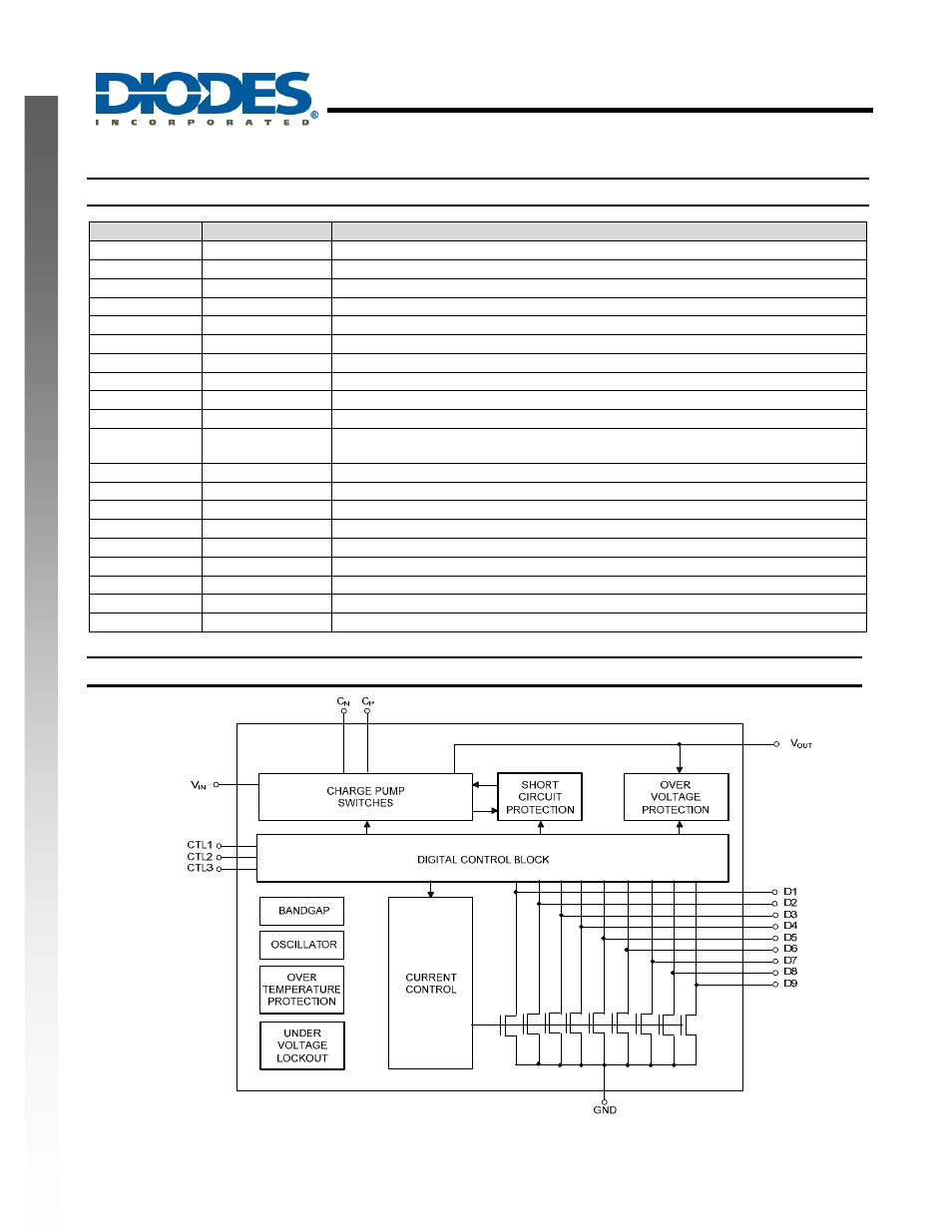
Functional Block Diagram