Ap1690, Absolute maximum ratings, Fb cs pd vcc out gnd – Diodes AP1690 User Manual
Page 3
AP1690
Document number: DS36469 Rev.
2 - 2
3 of 9
May 2014
© Diodes Incorporated
AP1690
A Product Line of
Diodes Incorporated
N
E
W
P
R
O
D
U
C
T
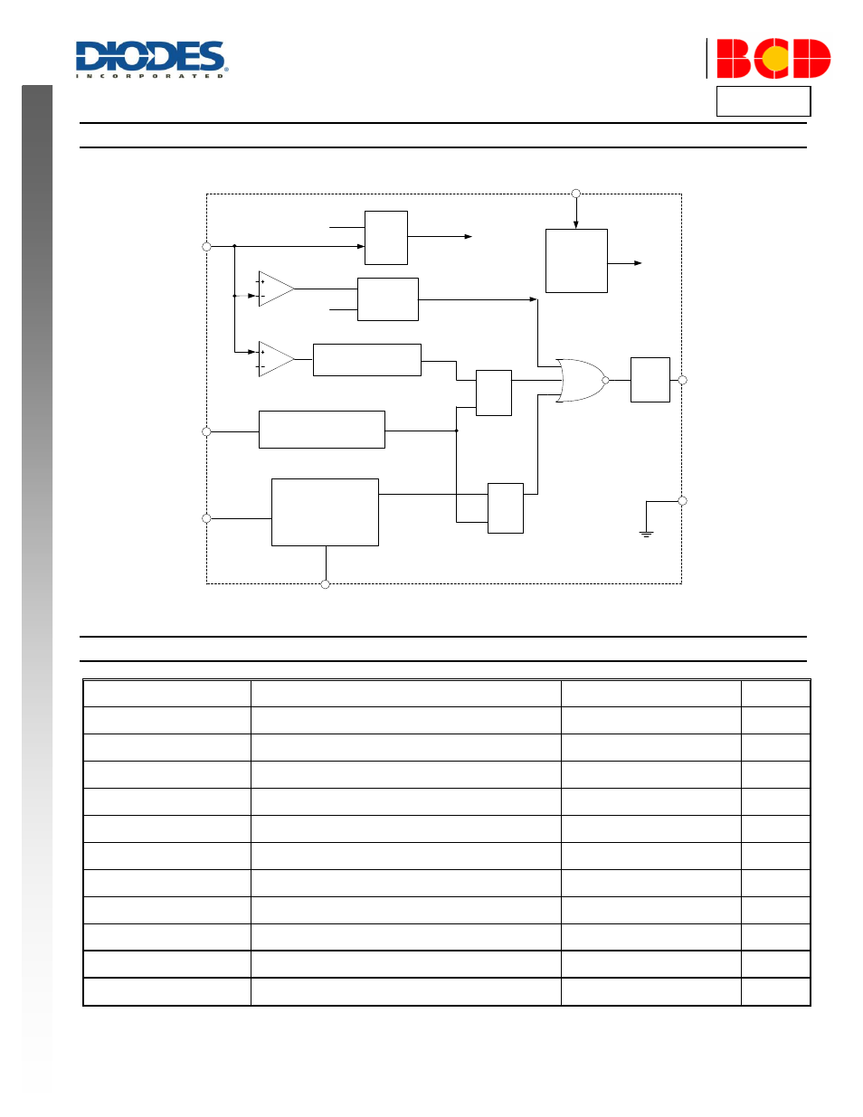
Functional Block Diagram
Regulator
&
Bias
OVP
Tonsec
Detector
0.1V
1.8V
PFM
Tons
UVLO
COMP
EA
UVLO
pro
CV_CTRL
PFM
Driver
R
Q
S
R
Q
S
CC_CTRL
FB
CS
PD
VCC
OUT
GND
Acceleration Start
Control
Peak Current Control
& LEB
Dimming Control
DIM
2
3
4
5
6
7
8
Absolute Maximum Ratings
(Note 4)
Symbol
Parameter
Rating
Unit
V
CC
Power Supply Voltage
-0.3 to 30
V
I
OUT
Driver Output Current
300
mA
V
PD
, V
DIM
, V
CS
Voltage at PD, DIM, CS
-0.3 to 7
V
V
FB
FB Input Voltage
-40 to 10
V
T
J
Operating Junction Temperature
+150
ºC
T
STG
Storage Temperature
-65 to +150
ºC
T
LEAD
Lead Temperature (Soldering, 10 sec)
+300
ºC
P
D
Power Dissipation at T
A
= +50
C
0.65
W
θ
JA
Thermal Resistance (Junction to Ambient)
190
C/W
–
ESD (Machine Model)
200
V
–
ESD (Human Body Model)
3000
V
Note 4
: Stresses greater than those listed under “Absolute Maximum Ratings” may cause permanent damage to the device. These are stress ratings only, and
functional operation of the device at these or any other conditions beyond those indicated under “Recommended Operating Conditions” is not implied.
Exposure to “Absolute Maximum Ratings” for extended periods may affect device reliability.