Az1117c, Absolute maximum ratings, Recommended operating conditions – Diodes AZ1117C User Manual
Page 4: Electrical characteristics az1117c-adj
AZ1117C
Document number: DS36676 Rev.
2 - 2
4 of 21
January 2014
© Diodes Incorporated
AZ1117C
A Product Line of
Diodes Incorporated
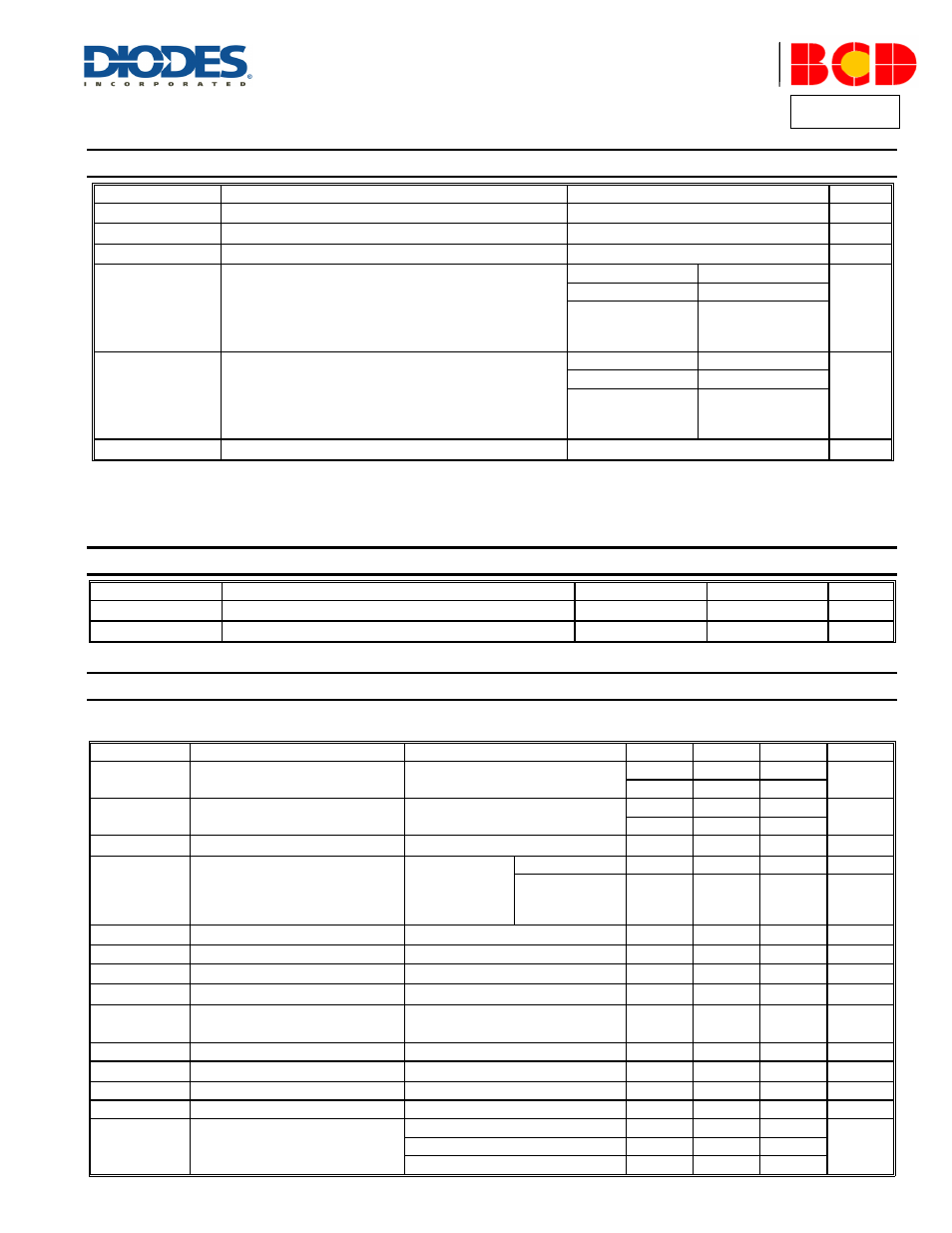
Absolute Maximum Ratings
(Note 5)
Symbol Parameter
Rating
Unit
V
IN
Input Voltage
18
V
T
J
Operating Junction Temperature Range
+150
°C
T
STG
Storage Temperature Range
-65 to +150
°C
θ
JA
Thermal Resistance (Without Heatsink)
SOT89-3L 170
°C/W
SOT223 125
TO2522 (3)/
TO2522 (4)/
TO2522 (5)
100
θ
JA
Thermal Resistance (With Heatsink) (Note 6)
SOT89-3L 150
°C/W
SOT223 100
TO2522 (3)/
TO2522 (4)/
TO2522 (5)
70
T
LEAD
Lead Temperature (Soldering, 10sec)
+260
°C
Notes: 5. Stresses greater than those listed under “Absolute Maximum Ratings” may cause permanent damage to the device. These are stress ratings only, and
functional operation of the device at these or any other conditions beyond those indicated under “Recommended Operating Conditions” is not implied.
Exposure to “Absolute Maximum Ratings” for extended periods may affect device reliability.
6. Chip is soldered to 100mm
2
(10mm*10mm) copper (top side solder mask) on 2oz.2 layers FR-4 PCB with 8*0.5mm vias.
Recommended Operating Conditions
Symbol Parameter
Min
Max
Unit
V
IN
Input Voltage
–
15
V
T
J
Operating Junction Temperature Range
-20
+125
°C
Electrical Characteristics AZ1117C-ADJ
(Operating Conditions: V
IN
= V
OUT
+2V, I
OUT
= 10mA, T
J
= +25°C, unless otherwise specified. (P ≤ maximum power dissipation). Limits appearing
in Boldface type apply over the entire junction temperature range for operation, -20°C to +125°C.)
Symbol Parameter
Conditions Min
Typ
Max
Unit
V
REF
Reference Voltage
1.5V ≤ V
IN
-V
OUT
≤ 10V
1.238 1.250 1.262
V
1.225
1.250
1.270
V
RLINE
Line Regulation
1.5V ≤ V
IN
-V
OUT
≤ 10V
— 0.001 0.1
%
— — 0.2
V
RLOAD
Load Regulation
—
—
0.4
1.0
%
V
DROP
Dropout Voltage
∆V
REF
= 1%,
I
OUT
= 0.8A
— –
1.2
1.3
V
TO2522 (3)/
TO2522 (4)/
TO2522 (5)
– 1.3 1.4 V
I
LIMIT
Current Limit
—
1
1.35
—
A
—
Adjust Pin Current
—
—
60
120
µA
—
Adjust Pin Current Change
1.5 ≤ (V
IN
-V
OUT
) ≤ 10V
— 0.2 5
µA
—
Minimum Load Current
1.5 ≤ (V
IN
-V
OUT
) ≤ 10V
— 1.7 5
mA
PSRR Ripple
Rejection
f = 120Hz, C
OUT
= 22µF
(V
IN
-V
OUT
) = 3V, I
OUT
= 300mA
—
70 — dB
— Temperature
Stability
–
—
0.5 — %
—
RMS Output Noise (% of V
OUT
) T
A
= +25°C, 10Hz ≤ f ≤ 10KHz
— 0.003 — %
—
Thermal Shutdown
Junction Temperature
—
+160
—
°C
— Thermal
Shutdown
Hysteresis
–
— +16 — °C
θ
JC
Thermal Resistance
(Junction to Case)
SOT89-3L —
30
—
°C/W
SOT223 —
15
—
TO2522(3) /TO2522(4) /TO2522(5)
—
10
—