Electrical characteristics, Ap7361 – Diodes AP7361 User Manual
Page 5
AP7361
Document number: DS33626 Rev. 9 - 2
5 of 22
October 2013
© Diodes Incorporated
AP7361
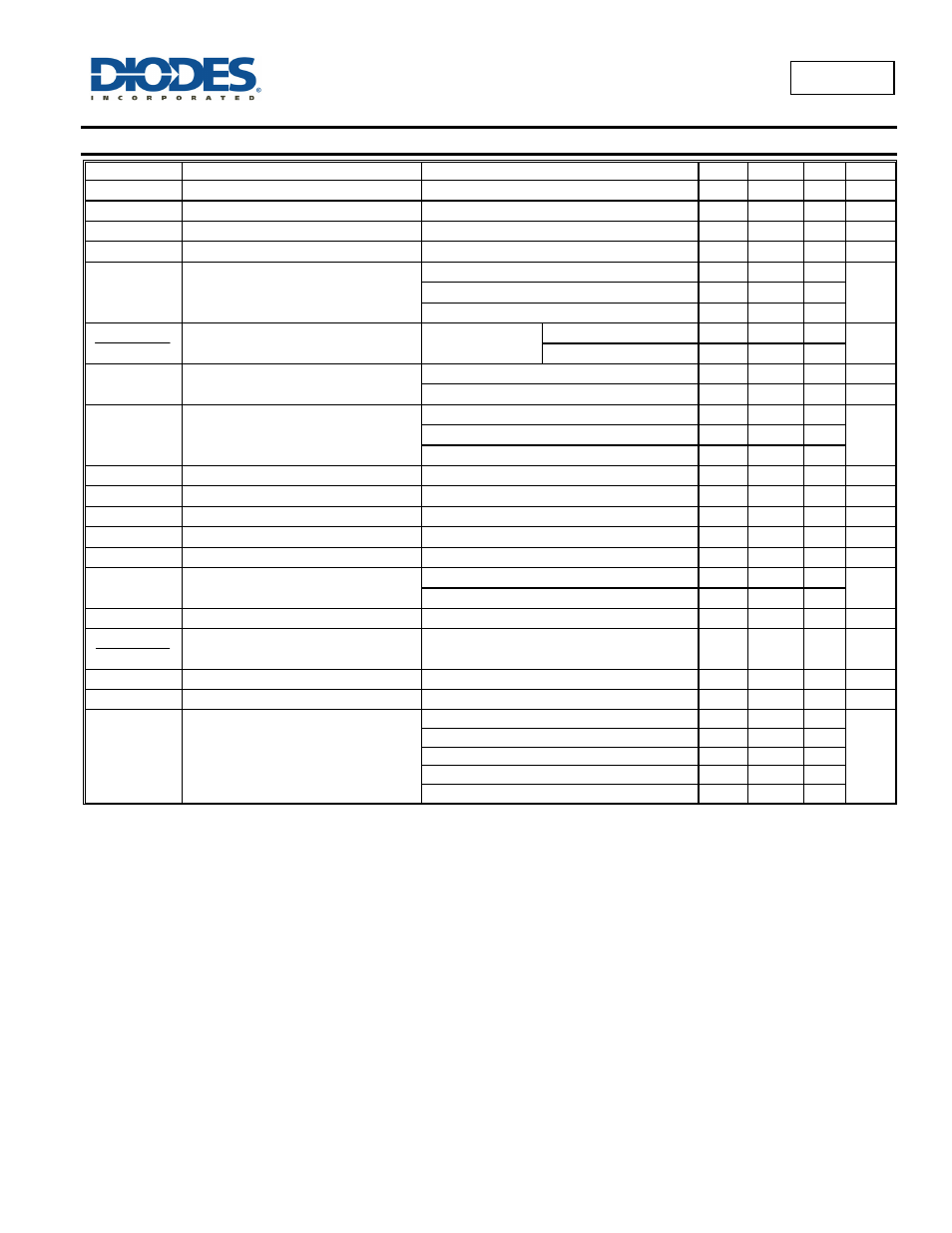
Electrical Characteristics
(@T
A
= +25°C, V
IN
= V
OUT
+1V, C
IN
= 1μF, C
OUT
= 4.7μF, V
EN
= V
IN
unless otherwise specified.)
Symbol Parameter
Test
Conditions
Min
Typ
Max
Unit
V
REF
FB Reference Voltage
I
OUT
= 10mA, T
A
= +25°C
0.8 V
I
ADJ
ADJ Pin Leakage
0.1
0.5
µA
I
Q
Input Quiescent Current
Enabled, I
OUT
= 0A
70
90
µA
I
SHDN
Input Shutdown Current
V
EN
= 0V, I
OUT
= 0A
-1 0.05 1 µA
V
OUT
Output Voltage Accuracy
I
OUT
= 100mA, T
A
= +25°C
-1 1
%
I
OUT
= 100mA, -40°C ≤ T
A
≤ +85°C
-2 2
Over V
IN
, I
OUT
, and T
A
-3 ±0.5 3
OUT
V
ΔVIN
ΔVOUT
Line Regulation
V
IN
= V
OUT
+1V to
6V, I
OUT
= 100mA
T
A
= +25°C
0.01
0.1
%/V
-40°C ≤T
A
≤ +85°C
0.2
V
OUT
/ V
OUT
Load Regulation
I
OUT
from 1mA to 300mA
-1.0 0.5 1.0 %
I
OUT
from 1mA to 1A
-1.0 0.5 1.0 %
V
DROPOUT
Dropout Voltage (Note 7)
I
OUT
= 300mA
150
200
mV
I
OUT
= 500mA
250
350
I
OUT
= 1A
500
700
V
IL
EN Input Logic Low Voltage
0
0.3
V
V
IH
EN Input Logic High Voltage
1.0
V
IN
V
I
EN
EN Input Leakage
V
IN
= 6V, V
EN
= 0V or 6V
-0.1 0.01 0.1 µA
I
LIMIT
Current Limit
V
IN
= V
OUT
+1V
1.1 1.5
A
I
SHORT
Short-Circuit Current
V
IN
= V
OUT
+1V, Output Voltage < 15% V
OUT
200 mA
PSRR
Power Supply Rejection Ratio
(Note 8)
f = 1KHz, I
OUT
= 100mA
60 65
dB
f = 10KHz, I
OUT
= 100mA
45
t
ST
Start-Up Time
V
OUT
= 3V, C
OUT
= 1µF, R
L
= 30Ω
200 µs
VOUT
A
ΔT
ΔVOUT
Output Voltage Temperature Coefficient
I
OUT
= 100mA, -40°C ≤ T
A
≤ +85°C
±130
ppm/°C
T
SHDN
Thermal Shutdown Threshold
150
°C
T
HYS
Thermal Shutdown Hysteresis
20
°C
θ
JA
Thermal Resistance Junction-to-Ambient
U-DFN3030-8 (Note 9)
70
°C/W
TO252 (Note 9)
95
SOT223 (Note 9)
110
SOT89-5 (Note 9)
150
SO-8EP (Note 9)
100
Notes:
7. Dropout voltage is the voltage difference between the input and the output at which the output voltage drops 2% below its
nominal value. This parameter only applies to output voltages above 1.5V since minimum V
IN
= 2.2V.
8. For V
IN
2.5V and V
IN
= V
OUT
+1V. For V
IN
< 2.5V, the PSRR performance may be reduced.
9. Test condition : DFN3030E-8, SO-8EP device mounted on 2"x2", FR-4 substrate PCB, with minimum recommended pad on top layer and thermal vias to
bottom layer ground plane. TO252 device mounted on 2"x2" FR-4 substrate PC board, 2oz copper, with minimum recommended pad layout.
SOT223 the device is mounted on FR-4 substrate PC board, with minimum recommended pad layout. SOT89-5L device mounted on 1"x1" FR-4
substrate PC board, with minimum recommended pad layout