New prod uc t ap7176b, Typical applications circuit, Pin descriptions – Diodes AP7176B User Manual
Page 2: Functional block diagram
AP7176B
Document number: DS35818 Rev.3 - 2
2 of 14
April 2014
© Diodes Incorporated
NEW PROD
UC
T
AP7176B
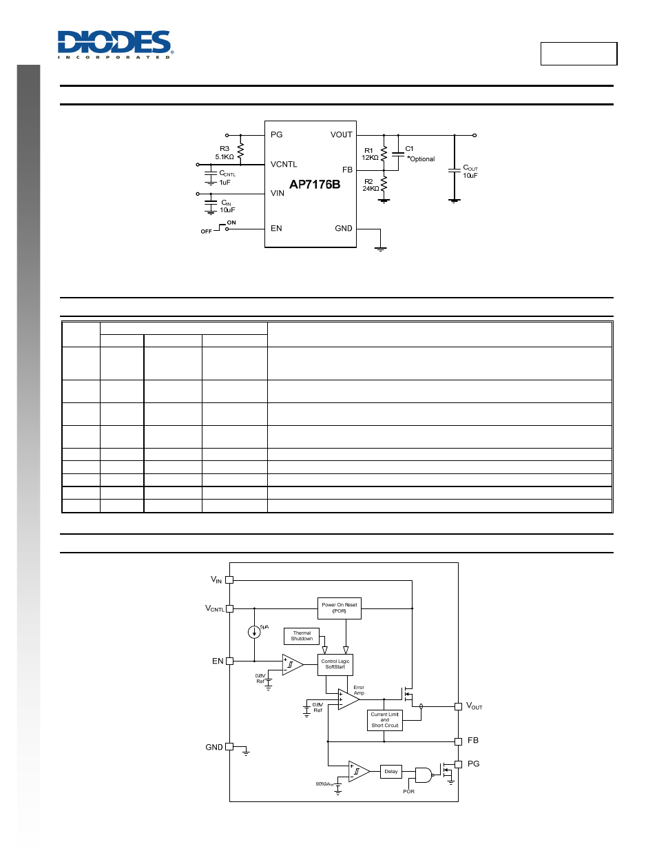
Typical Applications Circuit
Figure 1 Typical Application Circuit
Pin Descriptions
Pin
Name
Pin Number
Function
SO-8EP MSOP-8EP U-DFN3030-10
PG 1
1
5
Power Good.Output open drain to indicate the status of V
OUT
via monitoring the FB pin.
This pin is pulled low when the voltage is outside the limits, during thermal shutdown and
if either V
CNTL
or V
IN
go below their thresholds.
EN 2
2
6
Enable Pin. Driving this pin low will disable the part. When left floating an internal current
source will pull this pin high and enable it.
VIN 3
3
7,8,9
Power Input Pin for current supply. Connect a decoupling capacitor (≥10µF) as close as
possible to the pin for noise filtering
VCNTL 4
4
10
BIAS supply for the controller, recommended 5V. Connect a decoupling capacitor (≥1µF)
as close as possible to the pin for noise filtering.
NC 5
5
No
Connection
V
OUT
6
6
1,2,3
Power output pin
FB
7
7
4
Feedback to set the output voltage via an external resistor divider between V
OUT
and GND
GND 8
8
11 Ground
PAD
EP
EP
EP
Exposed pad connected to GND for good thermal conductivity
Functional Block Diagram