New prod uc t ap7176b, Application information, Layout consideration – Diodes AP7176B User Manual
Page 10

AP7176B
Document number: DS35818 Rev.3 - 2
10 of 14
April 2014
© Diodes Incorporated
NEW PROD
UC
T
AP7176B
Application Information
(cont.)
Output Capacitor
An output capacitor (C
OUT
) is needed to improve transient response and maintain stability. The ESR (equivalent series resistance) and
capacitance drives the selection. Care needs to be taken to cover the entire operating temperature range.
The output capacitor can be an Ultra-Low-ESR ceramic chip capacitor or a low ESR bulk capacitor like a solid tantalum, POSCap or aluminum
electrolytic capacitor.
C
OUT
is used to improve the output stability and reduces the changes of the output voltage during load transitions. The slew rate of the current
sensed via the FB pin in AP7176B is reduced. If the application has large load variations, it is recommended to utilize low-ESR bulk capacitors.
It is recommended to place ceramic capacitors as close as possible to the load and the ground pin and care should be taken to reduce the
impedance in the layout.
Input Capacitor
To prevent the input voltage from dropping during load steps it is recommended to utilize an input capacitor (C
IN
). As with the output capacitor
the following are acceptable, Ultra-Low-ESR ceramic chip capacitor or low ESR bulk capacitor like a solid tantalum, POSCap or aluminum
electrolytic capacitor. Typically it is recommended to utilize an capacitance of at least 10µF to avoid output voltage drop due to reduced input
voltage. The value can be lower if V
IN
changes are not critical for the application.
Layout Consideration
For good ground loop and stability, the input and output capacitors should be located close to the input, output, and ground pins of the device.
No other application circuit is connected within the loop. Avoid using vias within ground loop. If vias must be used, multiple vias should be used
to reduce via inductance.
The regulator ground pin should be connected to the external circuit ground to reduce voltage drop caused by trace impedance. Ground plane is
generally used to reduce trace impedance.
Wide trace should be used for large current paths from V
IN
to V
OUT
, and load circuit.
Place the R1, R2, and C1 (optional) near the LDO as close as possible to avoid noise coupling.
R2 is placed close to device ground. Connect the ground of the R2 to the GND pin by using a dedicated trace.
Connect the pin of the R1 directly to the load for Kelvin sensing.
No high current should flow through the ground trace of feedback loop and affect reference voltage stability.
For the packages with exposed pads, heat sinking is accomplished using the heat spreading capability of the PCB and its copper traces.
Suitable PCB area on the top layer and thermal vias (0.3mm drill size with 1mm spacing, 4 to 8 vias at least) to the V
IN
power plane can help to
reduce device temperature greatly.
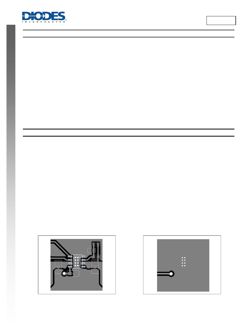
Reference Layout Plots:
Top Layer
Bottom Layer
GND
Vcntl
Vout
EN
Cin
Cout
FB
R1
R2
PG
1
C1
Ccntl
Vin
Vcntl
GND
GND
