Ap2280, Electrical characteristics, Single channel slew rate controlled load switch – Diodes AP2280 User Manual
Page 4
AP2280
Single Channel Slew Rate Controlled Load Switch
AP2280 Rev. 6
4 of 12
FEBRUARY 2009
©
Diodes Incorporated
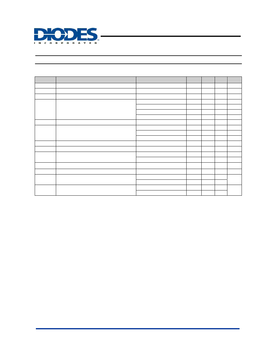
(T
A
= 25
o
C, V
IN
= V
EN
= 5.0V, unless otherwise stated)
Symbol
Parameters
Test Conditions
Min
Typ. Max
Unit
I
Q
Input Quiescent Current
V
EN
= V
IN
, I
OUT
= 0
⎯
0.004 1
μA
I
SHDN
Input Shutdown Current
V
EN
= 0V, OUT open
⎯
0.004 1
μA
I
LEAK
Input Leakage Current
V
EN
= 0V, OUT grounded
⎯
0.01 1
μA
R
DS(ON)
Switch on-resistance
V
IN
= 5.0V
80
105
m
Ω
V
IN
= 3.3V
92
120
m
Ω
V
IN
= 1.8V
150
200
m
Ω
V
IN
= 1.5V
200
250
m
Ω
V
IL
EN Input Logic Low Voltage
V
IN
= 1.5V to 6V
0.4
V
V
IH
EN Input Logic High Voltage
1.5V ≤ V
IN
≤ 2.7V
1.4 V
2.7V < V
IN
< 5.25V
1.6
V
V
IN
≥ 5.25V
1.7 V
I
SINK
EN Input leakage
V
EN
= 5V
⎯
1
μA
T
D(ON)
Output turn-on delay time
R
load
=10
Ω
1
μS
T
ON
Output turn-on rise time
AP2280-1, R
load
=10
Ω
100
150
μS
AP2280-2, R
load
=10
Ω
1000
1500
μS
T
D(OFF)
Output turn-off delay time
R
load
=10
Ω
0.4
1
μS
R
DISCH
Discharge FET on-resistance
V
EN
= GND
20
40
Ω
θ
JA
Thermal Resistance Junction-to-Ambient
SOT25 (Note 5)
160
o
C/W
DFN2018-6 (Note 6)
93
θ
JC
Thermal Resistance Junction-to-case
SOT25 (Note 5)
38
o
C/W
DFN2018-6 (Note 6)
41
Notes: 5. Test condition for SOT25: Device mounted on FR-4 substrate PC board, with minimum recommended pad layout.
6. Test condition for DFN2018-6: Device mounted on FR-4 2-layer board, 2oz copper, with minimum recommended pad on top layer and 3 vias to
bottom layer 1.0"x1.4" ground plane.
Electrical Characteristics