Ap2280, Block diagram, Pin assignments – Diodes AP2280 User Manual
Page 2: Pin description
AP2280
Single Channel Slew Rate Controlled Load Switch
AP2280 Rev. 6
2 of 12
FEBRUARY 2009
©
Diodes Incorporated
(1) SOT25
(2) DFN2018-6
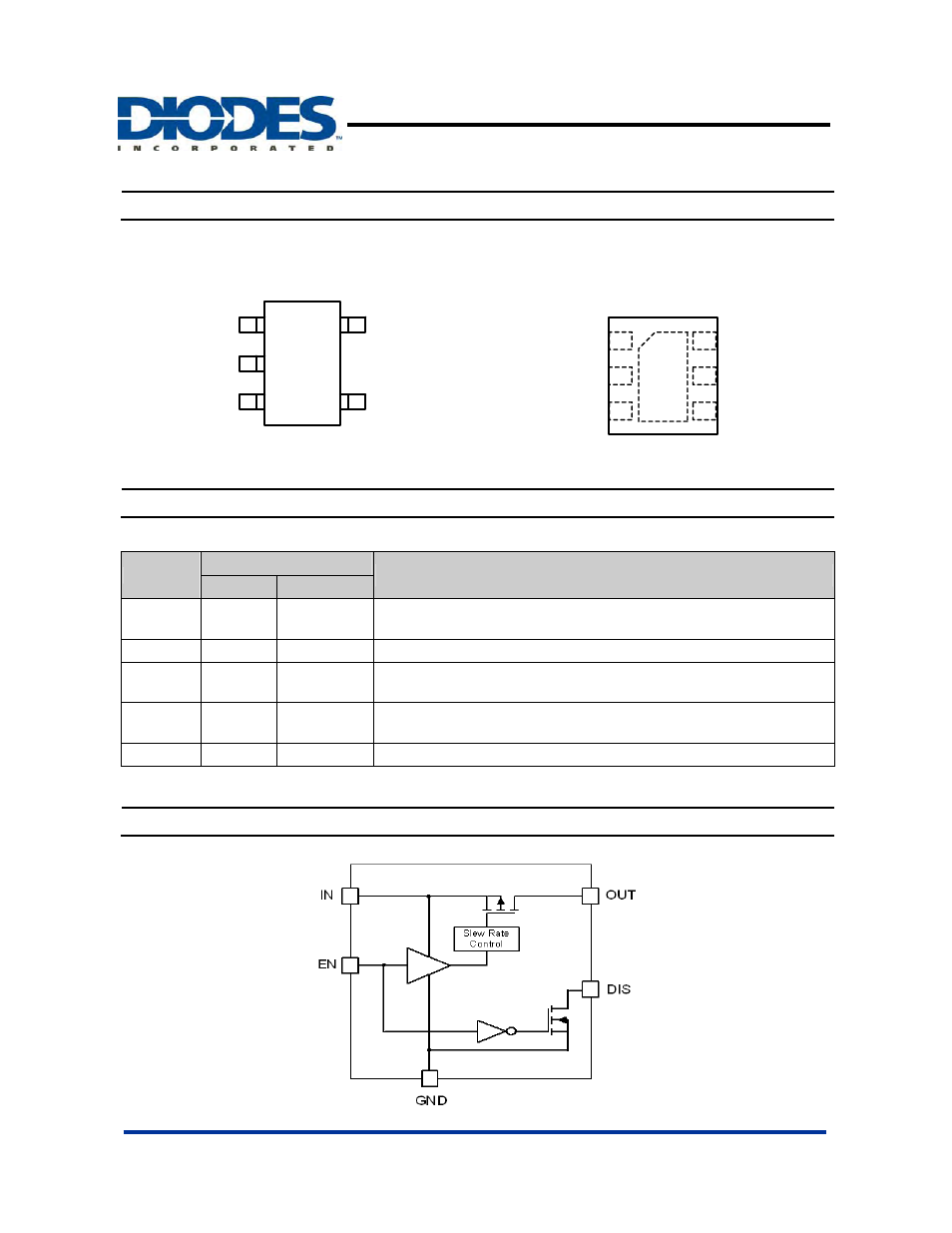
DIS
GND
OUT
IN
EN
( Top View )
5
4
3
2
1
OUT
GND
DIS
1
2
3
6
5
4
IN
IN
EN
( Top View )
Pin Name
Pin Number
Description
SOT25
DFN2018-6
DIS
1
3
Discharge pin. If DIS pin is tied to OUT pin externally, the output voltage
will be discharged to ground when disabled.
GND
2
2
Ground.
OUT
3
1
Voltage output pin. This is the pin to the P-channel MOSFET drain.
Bypass to ground through a 0.1uF capacitor.
IN
4
5, 6
Voltage input pin. This is the pin to the P-channel MOSFET source.
Bypass to ground through a 1µF capacitor.
EN
5
4
Enable input, active high
Block Diagram
Pin Assignments
Pin Description
See also other documents in the category Diodes Hardware:
- PDS3200 (5 pages)
- PDS340 (5 pages)
- PDS340Q (5 pages)
- PDS360 (5 pages)
- PDS360Q (5 pages)
- PDS4150 (4 pages)
- PDS3100Q (5 pages)
- PDS3100 (5 pages)
- PDS1240CTL (5 pages)
- PDS1045 (5 pages)
- PDS1040L (5 pages)
- PDS1040CTL (5 pages)
- PDS1040 (5 pages)
- PD3S230L (5 pages)
- PD3S230H (3 pages)
- PDS5100Q (5 pages)
- PDS835L (5 pages)
- PDS760 (5 pages)
- PDS560 (5 pages)
- PDS540 (5 pages)
- PDS5100H (5 pages)
- PDS5100 (5 pages)
- PDS4200H (6 pages)
- SBL3060CTP (4 pages)
- SBL30L30CT (3 pages)
- SBL3045CTP (4 pages)
- SBL3040CTP (4 pages)
- SBL2060CTP (4 pages)
- SBL2030CT - SBL2060CT (3 pages)
- SBL2045CTP (4 pages)
- SBL1060CTP (4 pages)
- SBL1040CTP (4 pages)
- SBG3030CT - SBG3045CT (5 pages)
- SB520 - SB560 (3 pages)
- SB370 - SB3100 (3 pages)
- SB320 - SB360 (3 pages)
- SBR10U100CT (5 pages)
- SBR10U150CT (5 pages)
- SBR10A45SP5 (5 pages)
- SBR1060CT (5 pages)
- SBR1045SP5 (5 pages)
- SBR1045SD1 (4 pages)
- SBR1045D1 (5 pages)
- SBR1045CTL (4 pages)
- SBR1040CT (5 pages)