Electrical characteristics – Diodes AP2176 User Manual
Page 4
AP2166/ AP2176
Document number: DS31814 Rev. 3 - 2
4 of 17
April 2013
© Diodes Incorporated
AP2166/ AP2176
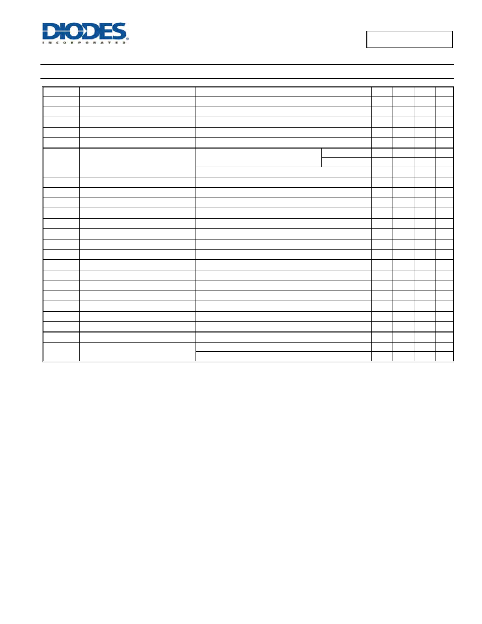
Electrical Characteristics
(@T
A
= +25°C, C
IN
= 10µF, V
IN
= +5V, unless otherwise specified.)
Symbol Parameter
Test
Conditions
Min
Typ
Max
Unit
V
UVLO
Input UVLO
R
LOAD
= 1k
Ω
1.6 1.9 2.5 V
I
SHDN
Input Shutdown Current
Disabled, I
OUT
= 0
0.5 1 µA
I
Q
Input Quiescent Current, Dual
Enabled, I
OUT
= 0
95
140
µA
I
LEAK
Input Leakage Current
Disabled, OUT grounded
1
µA
I
REV
Reverse Leakage Current
Disabled, V
IN
= 0V, V
OUT
= 5V, I
REV
at V
IN
1
µA
R
DS(ON)
Switch on-resistance
V
IN
= 5V, I
OUT
= 1A, -40°C
≤ T
A
≤ +85°C
MSOP-8EP
90
135
m
Ω
SO-8
100
135
m
Ω
V
IN
= 3.3V, I
OUT
= 1A, -40°C
≤ T
A
≤ +85°C
120
160
m
Ω
I
SHORT
Short-circuit current limit
Enabled into short circuit, C
L
= 68µF
1.5 A
I
LIMIT
Over-Load Current Limit
V
IN
= 5V, V
OUT
= 4.8V, C
L
= 120µF, -40°C
≤ T
A
≤ +85°C
1.1 1.5 1.9 A
I
Trig
Current limiting trigger threshold
V
IN
= V
EN
, Output Current Slew rate (<100A/WS), C
L
= 68µF
2.0 A
T
SHORT
Short-circuit response time
V
OUT
= 0V to I
OUT
= I
LIMIT
(short applied to output), C
L
= 68µF
20 µs
V
IL
EN Input Logic Low Voltage
V
IN
= 2.7V to 5.5V
0.8
V
V
IH
EN Input Logic High Voltage
V
IN
= 2.7V to 5.5V
2 V
I
SINK
EN Input leakage
V
EN
= 5V
1
µA
T
D(ON)
Output turn-on delay time
C
L
=1µF, R
LOAD
= 10
Ω
0.05 ms
T
R
Output turn-on rise time
C
L
=1µF, R
LOAD
= 10
Ω
0.6
1.5
ms
T
D(OFF)
Output turn-off delay time
C
L
=1µF, R
LOAD
= 10
Ω
0.01 ms
T
F
Output turn-off fall time
C
L
=1µF, R
LOAD
= 10
Ω
0.05
0.1
ms
R
FLG
FLG output FET on-resistance
I
FLG
=10mA
20
40
Ω
I
FOH
Error Flag Iff Current
V
FLG
= 5V
0.01 1 µA
T
Blank
FLG blanking time
C
L
= 68µF
4 7 15
ms
T
SHDN
Thermal shutdown threshold
Enabled, R
LOAD
= 1k
Ω
140
C
T
HYS
Thermal shutdown hysteresis
25
C
θ
JA
Thermal Resistance Junction-to-Ambient
SO-8
(Note
5)
110
o
C/W
MSOP-8EP (Note 6)
60
o
C/W
Notes:
5. Test condition for SO-8: Device mounted on FR-4 2-layer board, 2oz copper, with minimum recommended pad layout.
6. Test condition for MSOP-8EP: Device mounted on FR-4 2-layer board, 2oz copper, with minimum recommended pad on top layer and 3 vias to bottom
layer ground plane.