Pin descriptions, Functional block diagram – Diodes AP2176 User Manual
Page 2
AP2166/ AP2176
Document number: DS31814 Rev. 3 - 2
2 of 17
April 2013
© Diodes Incorporated
AP2166/ AP2176
Available Options
Part Number
Channel
Enable Pin
(EN)
Current Limit
(typ)
Recommended Maximum
Continuous Load Current
AP2166 2 Active
Low
1.5A
1.0A
AP2176 2 Active
High
1.5A
1.0A
Pin Descriptions
Pin Name
Pin Number
Function
SO-8 MSOP-8EP
EN1
1
1
Switch 1 enable input, active low (AP2166) or active high (AP2176)
FLG1
2
2
Switch 1 over-current and over-temperature fault report, open-drain
FLG2
3
3
Switch 2 over-current and over-temperature fault report, open-drain
EN2
4
4
Switch 2 enable input, active low (AP2166) or active high (AP2176)
OUT2
5
5
Switch 2 voltage output pin
GND 6 6
Ground
IN
7 7
Voltage
input
pin
OUT1
8
8
Switch 1 voltage output pin
Exposed Pad
—
Exposed Pad
Exposed Pad:
It should be connected externally to GND and thermal mass for enhanced thermal impedance.
It should not be used as electrical ground conduction path.
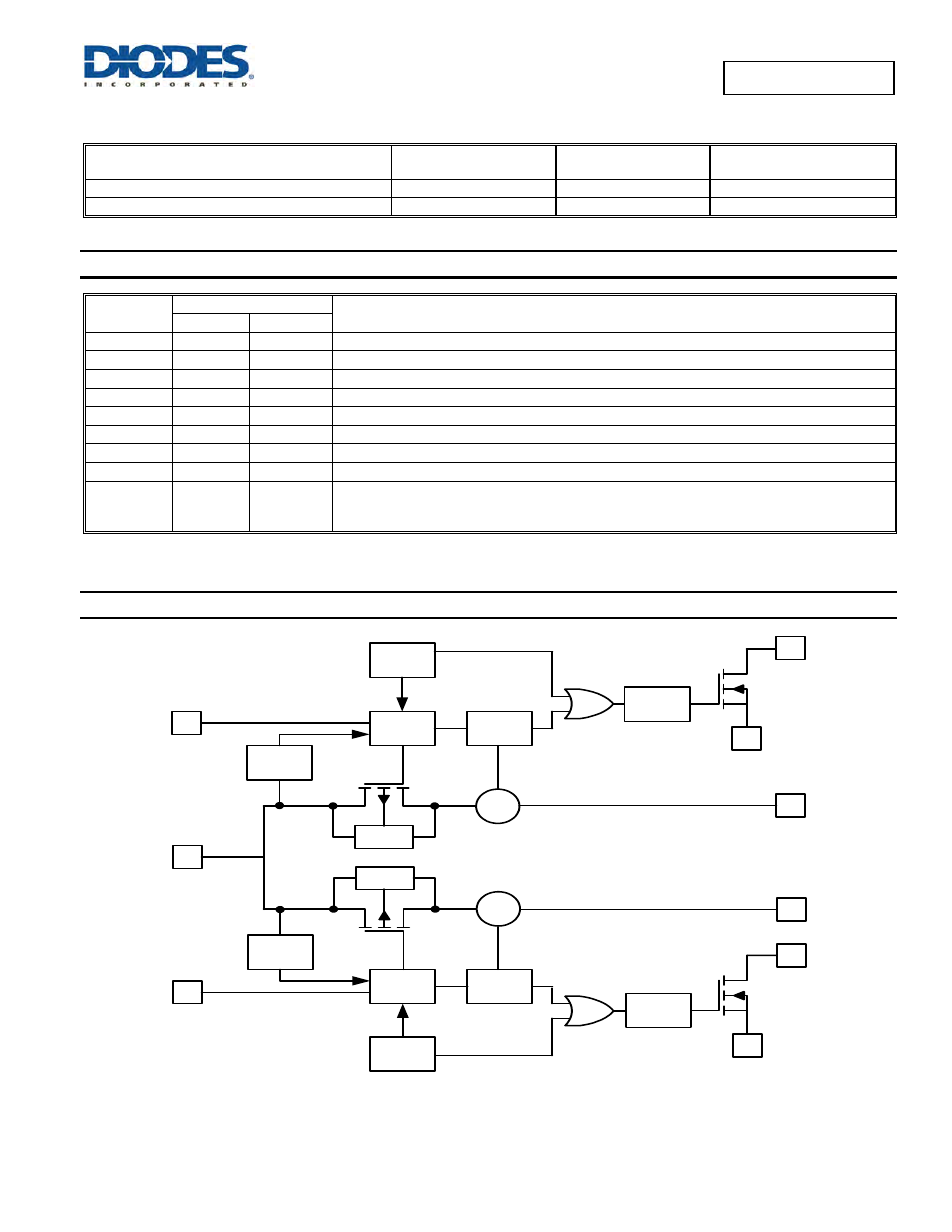
Functional Block Diagram
R e v e rs e
b lo c k in g
T h e r m a l
S e n s e
D riv e r
F L G 2
O U T 2
G N D
IN
E N 2
U V L O
C u rr e n t
L im it
C S
D e g litc h
R e v e r s e
b lo c k in g
T h e rm a l
S e n s e
D riv e r
U V L O
C u rre n t
L im it
C S
D e g litc h
O U T 1
F L G 1
E N 1
G N D