Data sheet, Pin configuration, Pin description – Diodes AUR9716 User Manual
Page 2
Data Sheet
1.0MHz to 1.4MHz, 2A, STEP DOWN DC-DC CONVERTER AUR9716
Apr. 2012 Rev. 1. 0 BCD Semiconductor Manufacturing Limited
2
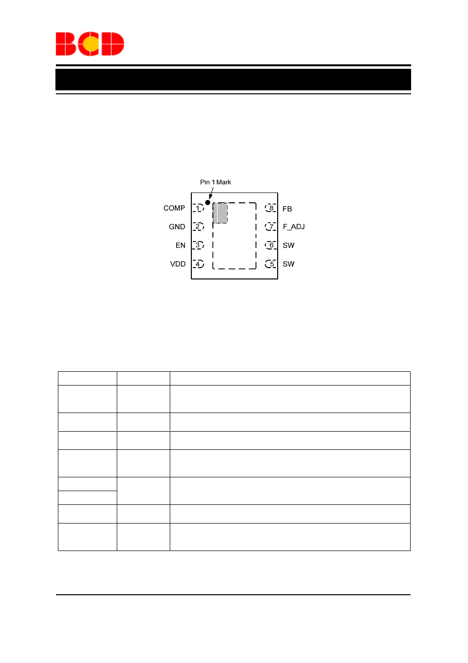
Pin Configuration
D Package
(DFN-3×3-8)
Figure 2. Pin Configuration of AUR9716 (Top View)
Pin Description
Pin Number
Pin Name
Function
1 COMP
Compensation Point. COMP is used to compensate the regulation control
loop. Connect R and C from COMP and GND to compensate the regulation
control loop
2 GND
Ground. The exposed pad is soldered to PCB and connected to GND plant
for good power dissipation
3 EN
Enable Input. EN is an input when the regulator on or off. When left
unconnected, EN pin is pulled to VDD by the internal pull up resistor
4 VDD
Power input V
IN
provides the input power to the regulator. Connecting a
ceramic bypass capacitor between VDD and GND to eliminate input
noise and ripple voltage
5
6
SW
Switch Output. SW is the switching point which supplies voltage and
current to output
7 F_ADJ
Oscillator Resistor Input. Connecting a resistor to ground from this pin sets
the switching frequency
8 FB
Feedback Input. Receives the feedback voltage from a resistive divider
connected across the output. The feedback reference voltage is 0.8V
typically