Data sheet, Application information (continued), F_adj : r – Diodes AUR9716 User Manual
Page 12: Selection, Thermal characteristics, Pc board layout considerations
Data Sheet
1.0MHz to 1.4MHz, 2A, STEP DOWN DC-DC CONVERTER AUR9716
Apr. 2012 Rev. 1. 0 BCD Semiconductor Manufacturing Limited
12
Application Information (Continued)
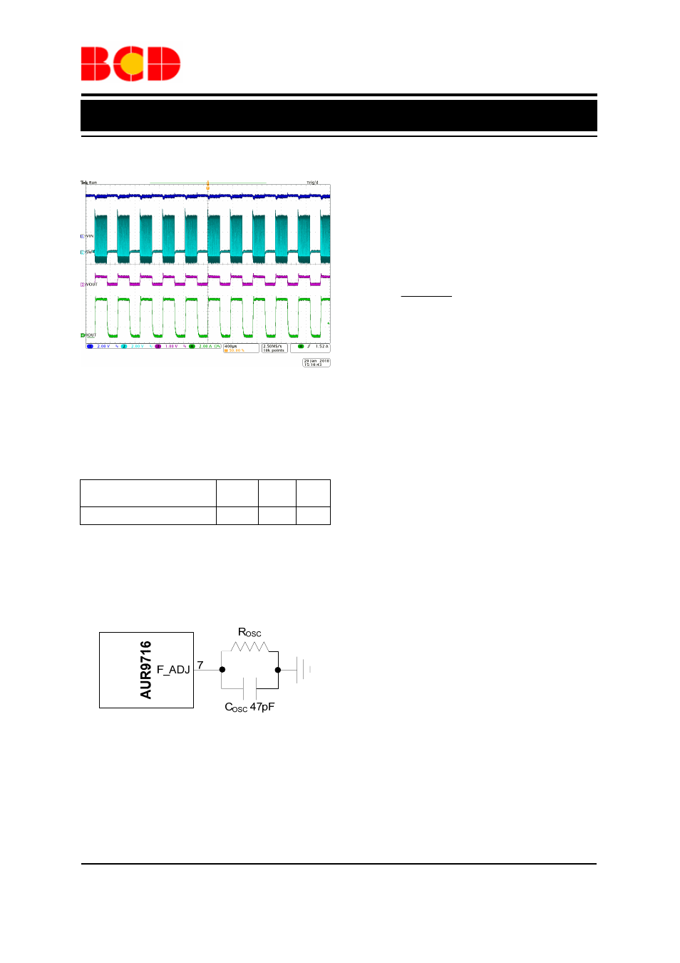
Figure 25. SCP Protection
7. F_ADJ : R
OSC
Selection
The AUR9716 can change switching frequency by
choose different R
OSC
, please refer to Table 2.
Switching Frequency
(MHz)
1.4 1.2 1.0
R
OSC
(kΩ) 5100
976
536
Table 2. R
OSC
Setting
Due to get the better performance of AUR9716,
F_ADJ pin (Pin 7)could parallel 47pF capacitor
with R
OSC
, shown in Figure 26.
Figure 26. F_ADJ Components
8. Thermal Characteristics
The max power dissipation depends on the thermal
resistance of IC package, PCB layout, the rate of
temperature between junction to ambient. The max
power dissipation can be calculated by following
formula:
⎟⎟
⎠
⎞
⎜⎜
⎝
⎛
−
=
JA
A
MAX
J
MAX
D
T
T
P
θ
)
(
)
(
Where T
J(max)
is the maximum operation junction
temperature, T
A
is the ambient temperature and θ
JA
is
the junction to ambient thermal resistance.
9. PC Board Layout Considerations
When laying out the printed circuit board, the
following checklist should be used to optimize the
performance of AUR9716.
1. The power traces, including the GND trace, the SW
trace and the
VDD trace should be kept direct, short
and wide.
2. To put the input capacitor as close as possible to the
VDD
and GND pins.
3. The FB pin should be connected directly to the
feedback resistor divider.
4. Keep the switching node, SW, away from the
sensitive FB pin and the node should be kept small
area.