Ap3436/a, Electrical characteristics – Diodes AP3436/A User Manual
Page 6
AP3436/A
Document number: DS37212 Rev.
2 - 2
6 of 15
April 2014
© Diodes Incorporated
AP3436/A
A Product Line of
Diodes Incorporated
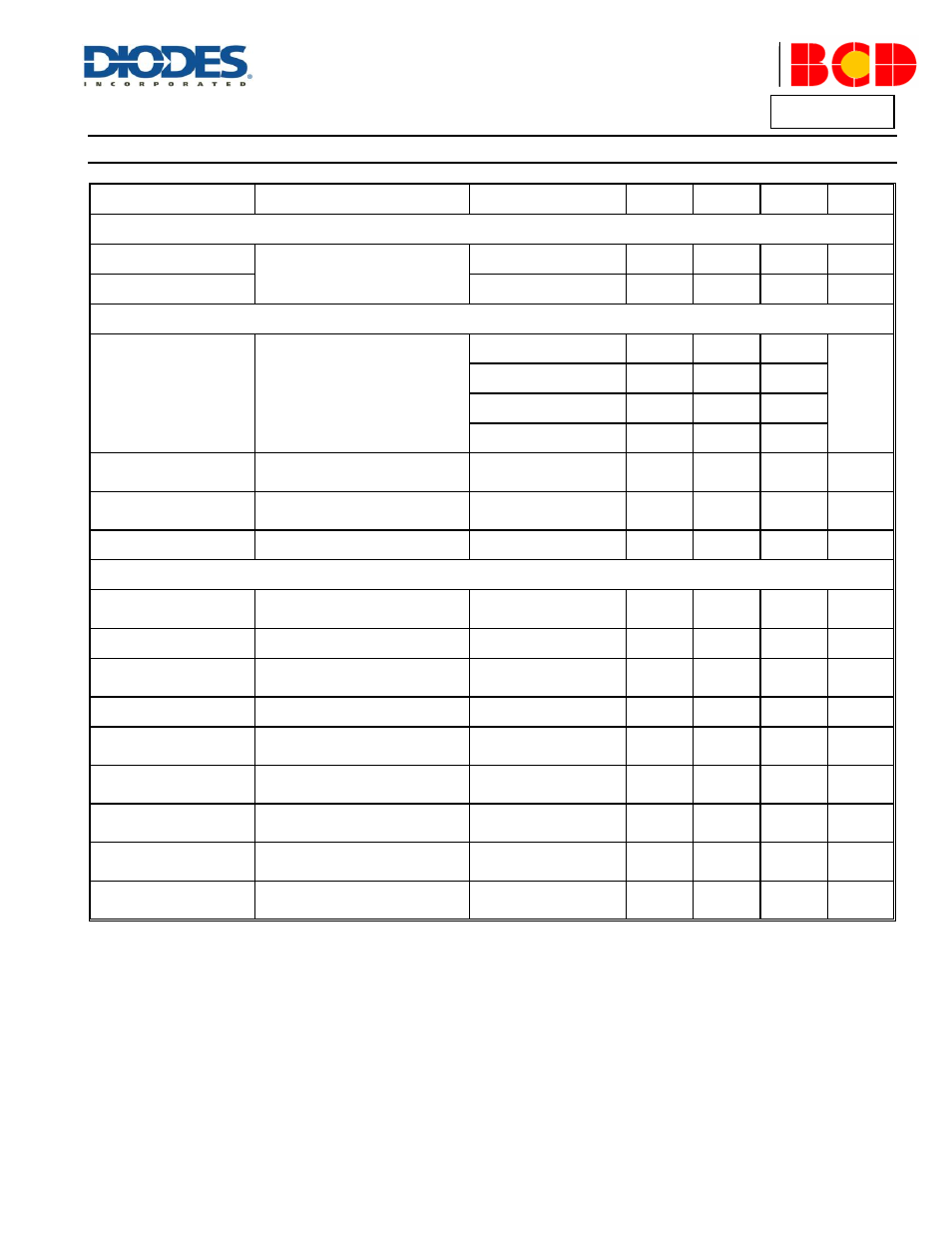
Electrical Characteristics
(Cont. V
CC
= 5V, V
IN
= 5V, T
A
= +25°C, unless otherwise specified.)
Symbol
Parameter
Conditions
Min
Typ
Max
Unit
ENABLE (EN PIN)
V
EN_L
EN Pin Threshold
–
–
–
0.8
V
V
EN_H
–
1.6
–
–
V
POWER GOOD (PGOOD PIN)
V
FBTH
Feedback Threshold
V
FB
falling (Fault)
70
75
–
%V
REF
V
FB
rising (Good)
77
82
–
V
FB
rising (Fault)
–
125
130
V
FB
falling (Good)
–
118
123
t
PG_DLY
Delay Time for PGOOD from High
to Low
–
–
30
–
µs
R
PG
Internal Power Good Pull Low
Resistance
–
–
–
150
Ω
R
PG_UP
External Pull-up Resistance Range
–
3000
–
–
Ω
SYSTEM PERFORMANCE
V
UVP
Output Under Voltage Protection
Threshold
V
IN
= 1.3 to 5.5V
–
–
0.5×
V
OUT
V
t
UVP
Delay Time for UVP Triggered
V
IN
= 1.5 to 5V
–
65
–
µs
V
OVP
Output Over Voltage Protection
Threshold
V
IN
= 1.3 to 5.5V
1.5×
V
OUT
–
–
V
t
OVP
Delay Time for OVP Triggered
V
IN
= 1.5 to 5V
–
65
–
µs
I
OUT
Output Current
V
IN
= 1.5 to 5V,
V
OUT
= 1.0V
3
–
–
A
–
Output Voltage Line Regulation
V
IN
= 1.5 to 5V,
I
OUT
= 100mA
–
0.4
–
%×
V
OUT
/V
–
Output Voltage Load Regulation
I
OUT
= 0A to 3A
–
0.3
–
%×
V
OUT
/A
V
TRAN
Output Voltage Load Transient
V
IN
= 5V, V
OUT
= 1.0V,
dI/dt = 400mA/µs
–
±2.5
–
%×
V
OUT
/A
η
Efficiency
V
CC
= 5V, V
IN
=5V,
I
OUT
= 3A, V
OUT
= 1.2V
–
80
–
%