Ap3436/a, Application information – Diodes AP3436/A User Manual
Page 10
AP3436/A
Document number: DS37212 Rev.
2 - 2
10 of 15
April 2014
© Diodes Incorporated
AP3436/A
A Product Line of
Diodes Incorporated
Application Information
1. Overview
The AP3436/A is a 3A synchronous buck (step-down) converter with two integrated N-channel MOSFETs. For AP3436, the regulator operates in
PWM mode with 1.25MHz switching frequency internally, regardless of if the load current is high or low. For AP3436A, when the load is very light,
the regulator automatically operates in the PSM mode to minimize the switching loss, thus achieving high efficiency at light load. When the load
increases, the regulator automatically switches over to a current-mode PWM operating at nominal 1.25MHz switching frequency.
2. Power On Reset
A Power On Reset (POR) circuitry continuously monitors the supply voltage at VCC pin. Once the rising POR threshold is exceeded, the
AP3436/A sets itself to active state and is ready to accept chip enable command. The rising POR threshold is typically 2.75V.
3. Soft Start
A built-in soft-start is used to prevent surge current from power supply input V
IN
during turn on (Referring to the Functional Block Diagram). The
error amplifier is a three-input device. Reference voltage V
REF
or the internal soft-start voltage V
SS
whichever is smaller dominates the behavior of
the non-inverting inputs of the error amplifier. V
SS
internally ramps up to 0.6V after the soft-start cycle is initiated. The ramp is created digitally, so
the output voltage will follow the V
SS
signal and ramps up smoothly to its target level.
4. EN Function
The AP3436/A provides Enable Function. Pulling this pin higher than 1.6V statically enables the AP3436/A while pulling the pin lower than 0.8V
statically for longer than 10µs will shutdown the IC.
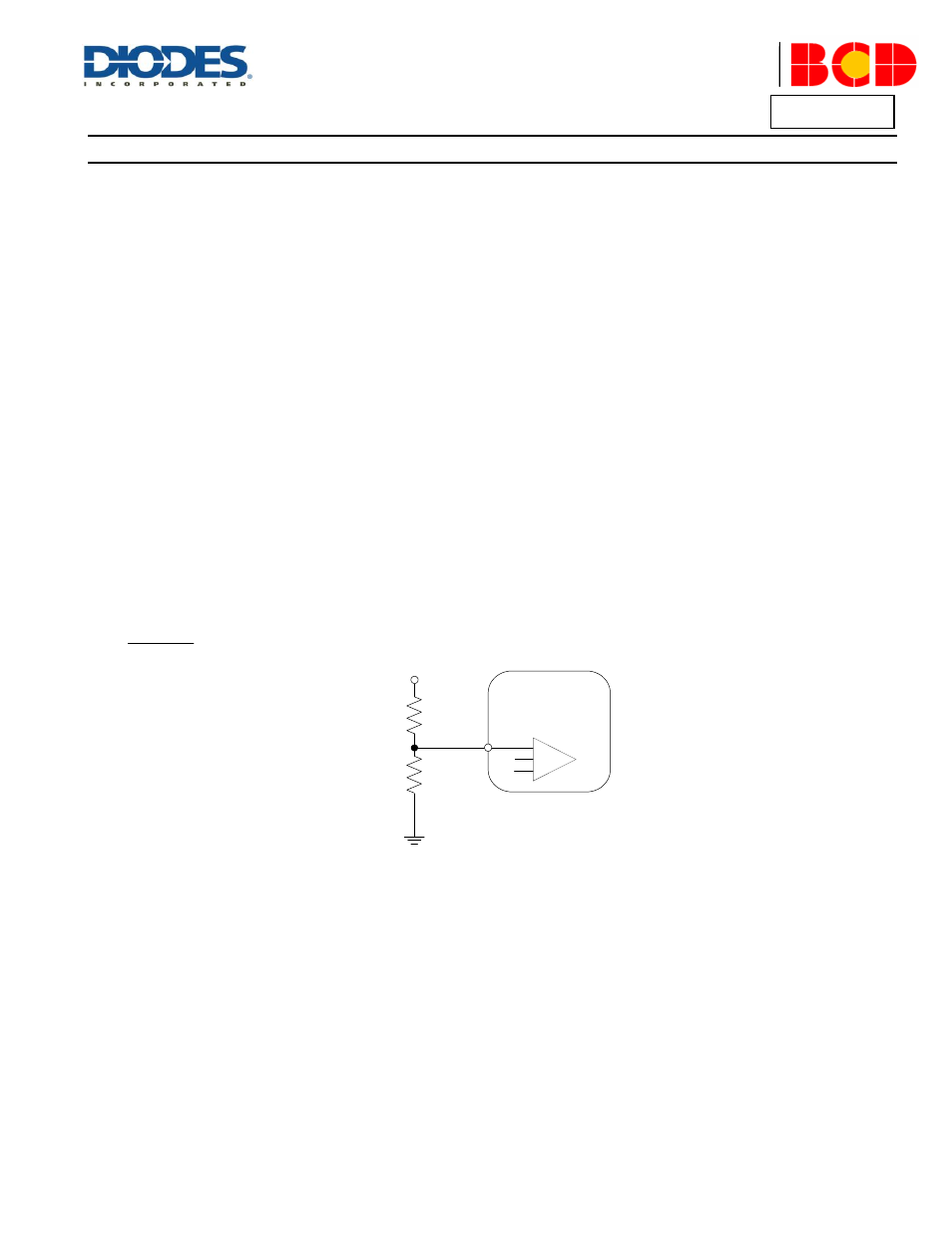
5. Adjusting Output Voltage
The output voltage is set with a resistor divider from the FB pin. It is recommended to use divider resistors with 1% tolerance or better. Start with a
100k
Ω for the resistor R1 and use the following equation to calculate R2. Consider using larger value resistors to improve efficiency at very light
loads. If the values are too high, the regulator is more susceptible to noise and the voltage errors caused by FB input current are noticeable.
Figure 1. Voltage Divider Circuit
6. Short Circuit Protection (SCP)
The AP3436/A has Over Current Protection (OCP) and Under Voltage Protection (UVP) functions.
6.1 OCP Function
The high side switch current is detected during each cycle. During SCP conditions, the output voltage is pulled down and the switch current is
increased. Once the increased high side switching current is detected to trigger the current limit of high side switch, the high side switch will be
immediately turned off and will not be turned on again until the next switching cycle. When over current condition is removed, the AP3436/A will
recover back to normal operation again.
6.2 UVP Function
The FB voltage is also monitored for Under Voltage Protection. The UV threshold is set at 0.2V. The under voltage protection has 65µs triggered
delay. When UVP is triggered, both high side and low side are shutdown immediately. The UVP is a latched function, reset power supply or EN pin
to restart AP3436/A again.
6
.
0
6
.
0
1
2
OUT
V
R
R
FB
V
OUT
R 1
R 2
AP3436/A
-
+
+
0.6V
V
SS