Ap3436/a, Absolute maximum ratings, Recommended operating conditions – Diodes AP3436/A User Manual
Page 4
AP3436/A
Document number: DS37212 Rev.
2 - 2
4 of 15
April 2014
© Diodes Incorporated
AP3436/A
A Product Line of
Diodes Incorporated
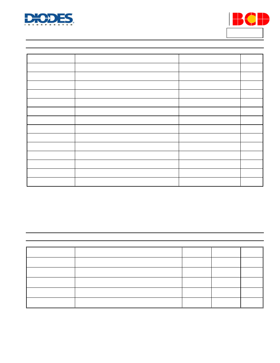
Absolute Maximum Ratings
(Note 5)
Symbol
Parameter
Rating
Unit
V
CC,
V
IN
VCC, VIN Pin Voltage
-0.3 to 6
V
V
EN
EN Pin Voltage
-0.3 to 6
V
V
SW
SW Pin Voltage
-0.3 to V
IN
+0.3
V
V
SW_TRANSIENT
SW Pin Transient Voltage (<50ns)
-5 to V
IN
+5
V
V
FB
FB Pin Voltage
-0.3 to 6
V
V
PGD
PGOOD Pin Voltage
-0.3 to 6
V
V
BOOT_SW
BOOT to SW Voltage
0 to 6
V
θ
JA
Thermal Resistance (Junction to Ambient, Simulation)
33
ºC/W
θ
JC
Thermal Resistance (Junction to Case)
3
ºC/W
T
J
Operating Junction Temperature
-40 to +150
ºC
T
STG
Storage Temperature
-65 to +150
ºC
T
LEAD
Lead Temperature (Soldering, 10sec)
+260
ºC
V
HBM
ESD (Human Body Model)
2000
V
V
MM
ESD (Machine Model)
200
V
Note 5:
Stresses greater than those listed under “Absolute Maximum Ratings” may cause permanent damage to the device. These are stress ratings only, and
functional operation of the dev
ice at these or any other conditions beyond those indicated under “Recommended Operating Conditions” is not implied.
Exposure to “Absolute Maximum Ratings” for extended periods may affect device reliability.
Recommended Operating Conditions
Symbol
Parameter
Min
Max
Unit
V
CC
Analog Input Voltage
3.0
5.5
V
V
IN
Power Input Voltage
1.3
5.5
V
I
OUT(MAX)
Maximum Output Current
3
–
A
V
OUT
Output Voltage
0.8
V
IN
V
T
A
Operating Ambient Temperature
-40
+85
ºC