Data sheet, Recommended operating conditions, Parameter symbol value unit – Diodes AP3431 User Manual
Page 4: Parameter symbol min max unit
Data Sheet
1.0MHz, 2.0A, Synchronous Step Down DC-DC Converter AP3431
Nov. 2011 Rev. 1. 0 BCD Semiconductor Manufacturing Limited
4
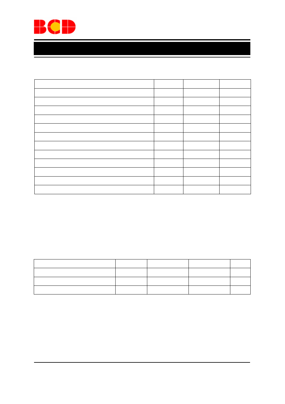
Absolute Maximum Ratings (Note 1)
Parameter
Symbol Value Unit
Supply Input for the Analog Circuit
V
CC
0 to 6.0
V
Power Supply Input for the MOSFET Switch
V
IN
0 to 6.0
V
SW Pin Switch Voltage
V
SW
-0.3 to V
IN
+0.3
V
Enable Voltage
V
EN
-0.3
to
V
IN
+0.3 V
SW Pin Switch Current
I
SW
2.9 A
Power Dissipation (on PCB, T
A
=25°C) P
D
1.45 W
Thermal Resistance (Junction to Ambient, Simulation)
θ
JA
68.63
°C/W
Junction Temperature
T
J
160 °C
Operating Temperature
T
OP
-40
to
85 °C
Storage temperature
T
STG
-55
to
150 °C
ESD (Human Body Model)
V
HBM
2000
V
ESD (Machine Model)
V
MM
200
V
Note 1: Stresses greater than those listed under “Absolute Maximum Ratings” may cause permanent damage to
the device. These are stress ratings only, and functional operation of the device at these or any other conditions
beyond those indicated under “Recommended Operating Conditions” is not implied. Exposure to “Absolute
Maximum Ratings” for extended periods may affect device reliability.
Recommended Operating Conditions
Parameter
Symbol Min
Max Unit
Supply Input Voltage
V
IN
2.7
5.5
V
Junction Temperature Range
T
J
-40
125
°C
Ambient Temperature Range
T
A
-40
80
°C