Preliminary datasheet, Functional block diagram – Diodes AP3408 User Manual
Page 3
Preliminary Datasheet
2A, 4MHz High Efficiency Synchronous Buck Converter AP3408
Jan. 2013 Rev. 1. 1
BCD Semiconductor Manufacturing Limited
3
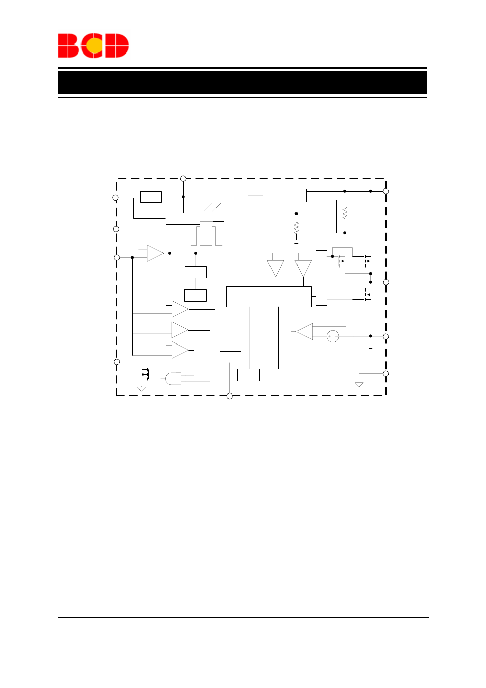
Functional Block Diagram
SD
Oscillator
SUM
CS
0.8V
EA
OCP
Dr
iver
Control
Logic
OTP
UVLO
V
REF
0.9V
SHDN/RT
PVDD
SW
GND
PGND
PGOOD
FB
COMP
1(1)
3(2)
10(8)
4(3)
5(4)
6(5)
8
9(7)
PWM
Clamp
SS
DC
SYNC
2
0.7V
0.4V
VDD
7(6)
A (B)
A for DFN-3X3-10
B for PSOP-8
Figure 3. Functional Block Diagram of AP3408
See also other documents in the category Diodes Hardware:
- PDS3200 (5 pages)
- PDS340 (5 pages)
- PDS340Q (5 pages)
- PDS360 (5 pages)
- PDS360Q (5 pages)
- PDS4150 (4 pages)
- PDS3100Q (5 pages)
- PDS3100 (5 pages)
- PDS1240CTL (5 pages)
- PDS1045 (5 pages)
- PDS1040L (5 pages)
- PDS1040CTL (5 pages)
- PDS1040 (5 pages)
- PD3S230L (5 pages)
- PD3S230H (3 pages)
- PDS5100Q (5 pages)
- PDS835L (5 pages)
- PDS760 (5 pages)
- PDS560 (5 pages)
- PDS540 (5 pages)
- PDS5100H (5 pages)
- PDS5100 (5 pages)
- PDS4200H (6 pages)
- SBL3060CTP (4 pages)
- SBL30L30CT (3 pages)
- SBL3045CTP (4 pages)
- SBL3040CTP (4 pages)
- SBL2060CTP (4 pages)
- SBL2030CT - SBL2060CT (3 pages)
- SBL2045CTP (4 pages)
- SBL1060CTP (4 pages)
- SBL1040CTP (4 pages)
- SBG3030CT - SBG3045CT (5 pages)
- SB520 - SB560 (3 pages)
- SB370 - SB3100 (3 pages)
- SB320 - SB360 (3 pages)
- SBR10U100CT (5 pages)
- SBR10U150CT (5 pages)
- SBR10A45SP5 (5 pages)
- SBR1060CT (5 pages)
- SBR1045SP5 (5 pages)
- SBR1045SD1 (4 pages)
- SBR1045D1 (5 pages)
- SBR1045CTL (4 pages)
- SBR1040CT (5 pages)