Preliminary datasheet, Pin configuration, Pin description – Diodes AP3408 User Manual
Page 2
Preliminary Datasheet
2A, 4MHz High Efficiency Synchronous Buck Converter AP3408
Jan. 2013 Rev. 1. 1
BCD Semiconductor Manufacturing Limited
2
1
2
3
4
8
7
6
5
SHDN/RT
GND
SW
PGND
PVDD
VDD
FB
COMP
Exposed Pad
Connected to
PGND
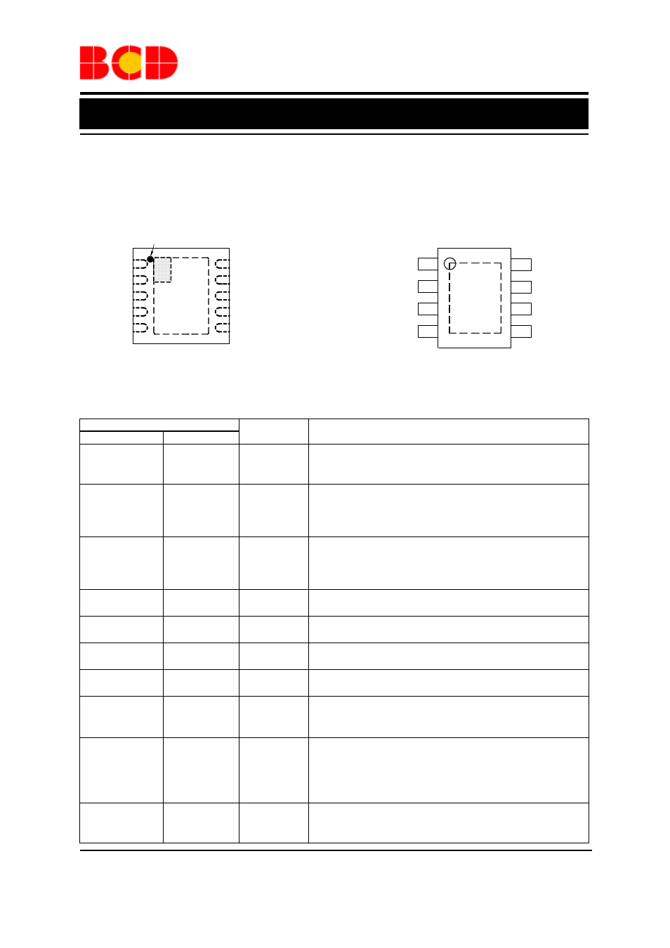
Pin Configuration
DN Package MP Package
(DFN-3×3-10) (PSOP-8)
Figure 2. Pin Configuration of AP3408 (Top View)
Pin Description
Pin Number
Pin Name
Description
DFN-3×3-10 PSOP-8
1 1
SHDN/RT
Oscillator resistor input. Connect a resistor to GND from
this pin to set the switching frequency. Forcing this pin to
V
DD
to shutdown the device
2
SYNC
External clock synchronization input. The oscillation
frequency can be synchronized to an external oscillation
applied to this pin. When tied to VDD, the internal
oscillator is selected
3 2
GND
Signal ground. All small-signal ground, such as the
compensation components and the exposed pad should be
connected to this pin, which in turn connects to PGND at
one point
4 3
SW
Internal power switch output. Connect this pin with one
terminal of the inductor
5 4
PGND
Power ground. Connect this pin as close as possible to CIN
and COUT
6 5
PVDD
Power input supply. Decouple this pin to PGND with a
capacitor
7 6
VDD
Signal input supply. Decouple this pin to GND with a
capacitor. Normally V
DD
is equal to V
PVDD
8
PGOOD
Power Good Indicator. Open-drain logic output that is
pulled to ground when the output voltage is not within ±
12.5% of regulation point
9 7
FB
Feedback voltage. This pin is the inverting input of internal
error amplifier. It senses the converter output voltage
through an external resistor divider. The internal reference
voltage is 0.8V, which determines the output voltage
through the resistor divider
10 8
COMP
Compensation input. This pin is the output of internal error
amplifier. Connect external compensation elements to this
pin to stabilize the control loop
SHDN/ RT
SYNC
GND
SW
PGND
COMP
FB
PGOOD
VDD
PVDD
Pin 1 Mark
1
2
3
4
5
6
7
8
9
10
Exposed Pad
Connected to
PGND