Ap1513, Electrical characteristics, Pwm control 2a step-down converter – Diodes AP1513 User Manual
Page 4
AP1513
PWM CONTROL 2A STEP-DOWN CONVERTER
AP1513 Rev. 4
4 of 9
JULY 2009
DS31053
www.diodes.com
©
Diodes Incorporated
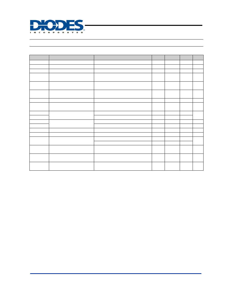
Electrical Characteristics
(V
IN
= 12V, T
A
= 25°C, unless otherwise specified)
Symbol
Parameter
Conditions
Min.
Typ.
Max.
Unit
V
FB
Feedback
Voltage
I
OUT
= 0.1A
0.784
0.8
0.816
V
I
FB
Feedback Bias Current
I
OUT
= 0.1A
-
0.1
0.5
µA
I
SW
Switch
Current
--
2.5 -
- A
I
SSS
Current Consumption
During Power Off
V
EN
= 0V
-
10
-
µA
∆V
OUT
/V
OUT
Line Regulation
V
IN
= 5V~18V
-
1
2
%
∆V
OUT
/V
OUT
Load Regulation
I
OUT
= 0.1 to 2A
-
0.2
0.5
%
f
OSC
Oscillation Frequency
Measure waveform at SW pin
240
300
400
KHz
f
OSC1
Frequency of Current Limit
or Short Circuit Protect
Measure waveform at SW pin
10
-
-
KHz
V
SH
EN Pin Input Voltage
Evaluate oscillation at SW pin
2.0
-
-
V
V
SL
Evaluate oscillation stop at SW pin
-
-
0.8
I
SH
EN Pin Input Leakage
Current
-- -
20
-
µA
I
SL
--
-
-10
-
µA
I
OCSET
OCSET Pin Bias Current
--
75
90
105
µA
T
SS
Soft-Start
Time
--
0.3
2
5
ms
R
DSON
Internal MOSFET Rdson
V
IN
= 5V, V
FB
= 0V
-
110
150
mΩ
V
IN
= 12V, V
FB
= 0V
-
70
100
EFFI Efficiency
V
IN
= 12V, V
OUT
= 5V
I
OUT
= 2A
- 92 - %
θ
JA
Thermal Resistance
Junction-to-Ambient
SOP-8L (Note 3)
-
134
-
o
C/W
θ
JC
Thermal Resistance
Junction-to-Case
SOP-8L (Note 3)
-
22
-
o
C/W
Notes: 3. Test conditions: Device mounted on FR-4 PCB, 2"*2", 2oz copper minimum recommended pad layout, single-sided, PC boards.