Data sheet, Function description – Diodes AP3586A/B/C User Manual
Page 12
Data sheet
Single Phase Synchronous Buck PWM Controller AP3586A/B/C
Mar. 2012 Rev. 1. 1 BCD Semiconductor Manufacturing Limited
12
Function Description
The AP3586A/B/C is a voltage-mode single phase
synchronous buck controller with embedded
MOSFET drivers. This part provides complete
protection functions such as over voltage protection,
under voltage protection and over current protection.
Inductor current information is sensed by R
DS(ON)
of
the low side MOSFET. The over current protection
threshold can be simply programmed by a resistor.
Power on Reset and Chip Enable
A power on reset (POR) circuitry continuously
monitors the supply voltage at VCC pin. Once the
rising POR threshold is exceeded, the AP3586A/B/C
sets itself to active state and is ready to accept chip
enable command. The rising POR threshold is
typically 4.2V at VCC rising.
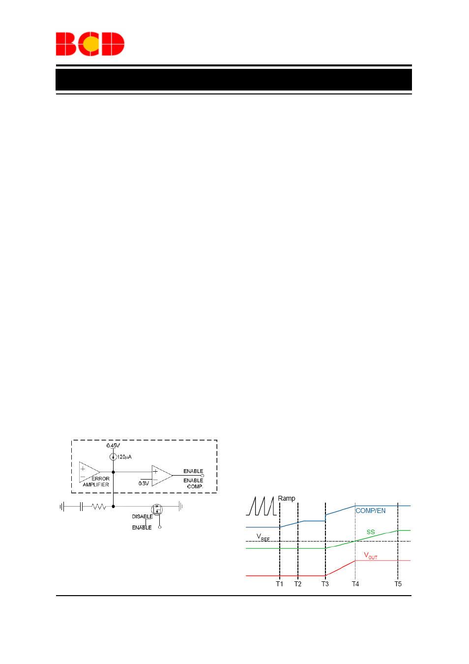
The COMP/EN is a multifunctional pin:
control loop compensation and chip enable as shown
in Figure 17. An Enable Comparator monitors the
COMP/EN pin voltage for chip enable. A signal level
transistor is adequate to pull this pin down to ground
and shut down AP3586. A 120
µ
A current source
charges the external compensation network with
0.45V ceiling when this pin is released. If the voltage
at COMP/EN pin exceeds 0.3V, the AP3586A/B/C
initiates its soft start cycle.
The 120
µ
A current source keeps charging the COMP
pin to its ceiling until the feedback loop boosts the
COMP pin higher than 0.45V according to the
feedback signal. The current source is cut off when
V
COMP
is higher than 0.45V during normal operation.
Figure 17. Chip Enable Function
Soft Start
A built-in Soft Start is used to prevent surge current
from power supply input V
IN
during turn-on
(Referring to the Functional Block Diagram). The
error amplifier is a three-input device. Reference
voltage V
REF
or the internal soft start voltage SS
whichever is smaller dominates the behavior of the
non-inverting inputs of the error amplifier. SS
internally ramps up to 0.6V in 2ms for AP3586A (to
0.8V in 2.7ms for AP3586B; to 0.8V in 3.6ms for
AP3586C) after the soft start cycle is initiated. The
ramp is created digitally, so there will be 100 small
discrete steps. Accordingly, the output voltage will
follow the SS signal and ramp up smoothly to its
target level.
The SS signal keeps ramping up after it exceeds the
internal 0.6V (0.8V for AP3586B/C) reference
voltage. However, the internal 0.6V(0.8V for
AP3586B/C) reference voltage takes over the
behavior of error amplifier after SS>V
REF
. When the
SS signal climbs to its ceiling voltage (4.2V),
AP3586A/B/C claims the end of soft start cycle and
enables the under voltage protection of the output
voltage.
Figure 18 shows a typical start up interval for
AP3586A/B/C where the COMP/EN pin has been
released from a grounded (system shutdown) state.
The internal 120
µ
A current source starts charge the
compensation network after the COMP/EN pin is
released from ground at T1. The COMP/EN exceeds
0.3V and enables the AP3586A/B/C at T2. The
COMP/EN continues ramping up the stays at 0.45V
before the SS starts ramping at T3. The output
voltage follows the internal SS and ramps up to its
final level during T3 and T4. At T4, the reference
voltage V
REF
takes over the behavior of the error
amplifier as the internal SS crosses V
REF
. The internal
SS keeps ramping up and stays at 4.2V at T5, where
AP3586A/B/C asserts the end of soft start cycle.