Maximum ratings, Thermal characteristics, Electrical characteristics – Diodes D5V0F4U10LP User Manual
Page 2
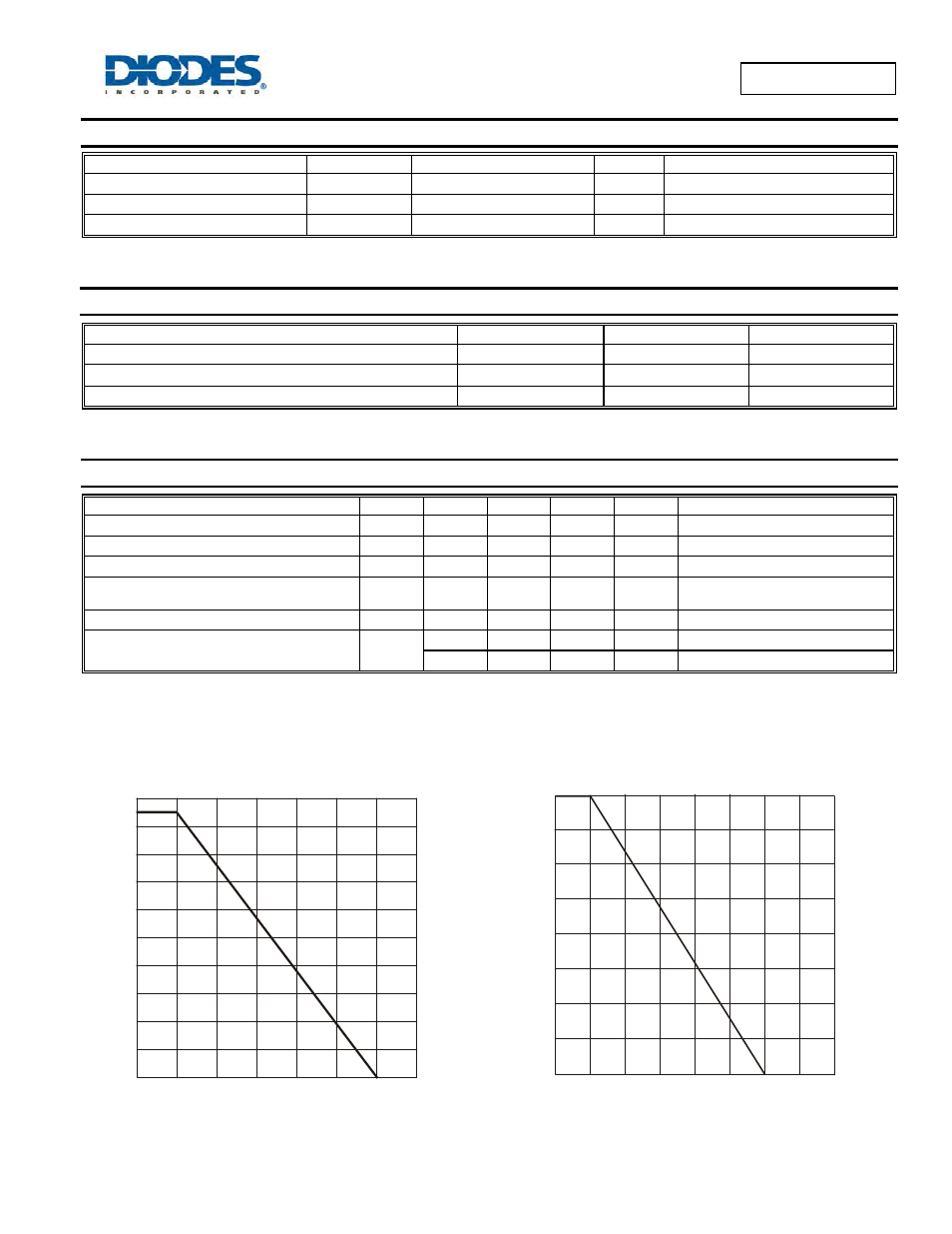
D5V0F4U10LP
Document number: DS35456 Rev. 3 - 2
2 of 4
July 2013
© Diodes Incorporated
D5V0F4U10LP
Maximum Ratings
(@T
A
= +25°C, unless otherwise specified.)
Characteristic Symbol Value Unit Conditions
Peak Pulse Current
I
PP
3.0 A
8/20µs, Figure 3
ESD Protection – Contact Discharge
V
ESD_Contact
±8 kV
Standard IEC 61000-4-2
ESD Protection – Air Discharge
V
ESD_Air
±15 kV
Standard IEC 61000-4-2
Thermal Characteristics
Characteristic Symbol
Value
Unit
Power Dissipation (Note 5)
P
D
380 mW
Thermal Resistance, Junction to Ambient T
A
= +25°C
R
JA
327 °C/W
Operating and Storage Temperature Range
T
J
, T
STG
-55 to +150
°C
Electrical Characteristics
(@T
A
= +25°C, unless otherwise specified.)
Characteristic
Symbol
Min
Typ
Max
Unit
Test Conditions
Reverse Working Voltage
V
RWM
—
—
5.5
V
—
Reverse Current (Note 6)
I
R
— — 200 nA
V
R
= 5.5V
Reverse Breakdown Voltage
V
BR
6.0 — — V
I
R
= 1mA
Reverse Clamping Voltage, Positive Transients
(Note 7)
V
CL
— 10 12 V
I
PP
= 1A, t
p
= 8/20
μs
Dynamic Resistance
R
DYN
— 1.0 —
Ω
I
R
= 1A, t
p
= 8/20
μs
Capacitance (Note 8)
C
T
— 0.4
0.65 pF
V
R
= 2.5V, f = 1MHz
— 0.5 — pF
V
R
= 0V, f = 1MHz
Notes:
5. Device mounted on FR-4 PCB pad layout (2oz copper) as shown on Diodes, Inc. suggested pad layout AP02001, which can be found on our website at
6. Short duration pulse test used to minimize self-heating effect.
7. Clamping voltage value is based on an 8x20µs peak pulse current (I
pp
) waveform.
8. Measured from any I/O pin to GND.
9. For information on the impact of Diodes' USB 2.0 compatible ESD protectors on signal integrity including eye diagram plots, please refer to AN77 at the
follow
0
125
175
T , AMBIENT TEMPERATURE ( C)
Figure 1 Power Derating Curve
A
°
P
,
P
O
WE
R
D
IS
S
IP
A
T
IO
N
(mW
)
D
25
100
50
75
150
0
40
80
120
160
200
Note 5
240
280
320
360
400
0
50
25
50
75
100
125
150
P
EAK
P
U
LS
E
D
E
R
A
T
IN
G
%
O
F
PE
AK P
O
W
E
R OR
CURRENT
T , AMBIENT TEMPERATURE (°C)
Figure 2 Pulse Derating Curve
A
0
100
25
75
175 200