Marking information, Absolute maximum ratings, Thermal characteristics – Diodes APT13003D User Manual
Page 2: Esd ratings
APT13003D
Datasheet Number: DS36347 Rev. 1 - 2
2 of 7
July 2013
© Diodes Incorporated
A Product Line of
Diodes Incorporated
APT13003D
Marking Information
Absolute Maximum Ratings
(@T
A
= +25°C, unless otherwise specified.)
Characteristic Symbol
Value
Unit
Collector-Emitter Voltage (V
BE
= 0V)
V
CES
700 V
Collector-Emitter Voltage
V
CEO
450 V
Emitter-Base Voltage
V
EBO
9 V
Continuous Collector Current
I
C
1.5 A
Peak Pulse Collector Current
I
CM
3 A
Continuous Base Current
I
B
0.75 A
Peak Pulse Base Current
I
BM
1.5 A
Thermal Characteristics
(@T
A
= +25°C, unless otherwise specified.)
Characteristic Symbol
Value
Unit
Power Dissipation
For TO92
P
D
1.1
W
For TO126@ T
C
= +25°C
20
For TO251@ T
C
= +25°C
24
Thermal Resistance, Junction to Ambient Air
For TO92
R
θJA
113.6
C/W
For TO126
96
For TO251
110
Thermal Resistance, Junction to Case
For TO92
R
θJC
83.3
C/W
For TO126
6.25
For TO251
5.0
Operating and Storage Temperature Range
T
J,
T
STG
-65 to +150
C
ESD Ratings
(Note 6)
Characteristic Symbol
Value
Unit
JEDEC
Class
Electrostatic Discharge - Human Body Model
ESD HBM
≥ 8,000
V
3B
Electrostatic Discharge - Machine Model
ESD MM
≥ 400
V
C
Note:
6. Refer to JEDEC specification JESD22-A114 and JESD22-A115.
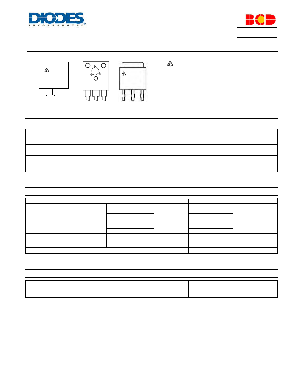
TO92
TO126
TO251
= Manufacturers’ code marking
For TO92, 13003DZ-G1 = Product Type Marking ID
For TO126, GU13003D = Product Type Marking ID
For TO251, APT13003DI-G1= Product Type Marking ID
YWW = Date Code Marking
e.g. 312 = Year 2013, Week 12.
8 = Assembly site code
XX = Batch Number
Flat Face
View
13003D
Z-G1
YWW8XX
GU13003D
YWW8XX
APT13003D
I-G1
YWW8XX
Front Face View
Front Face View