New prod uc t, Znbg4003, Device description – Diodes ZNBG4003 User Manual
Page 2: Typical application circuit
ZNBG4003
Document number: DS35007 Rev. 1 - 2
2 of 6
June 2012
© Diodes Incorporated
NEW PROD
UC
T
A Product Line of
Diodes Incorporated
ZNBG4003
Device Description
The ZNBG series of devices are designed to meet the bias
requirements of GaAs and HEMT FETs commonly used in
satellite receiver LNBs with a minimum of external components.
The ZNBG4003 provides four FET bias stages, arranged in two
pairs of two. Resistors connected to pins R
CAL
1 and R
CAL
2 set the
FET drain currents of each pair over the range of 0 to 15mA,
allowing input FETs to be biased for optimum noise and amplifier
FETs for optimum gain.
Drain voltages of all stages are set at 2.0V. The drain supplies are
current limited to approximately 5% above the operating currents
set by the Rcal resistors.
Depletion mode FETs require a negative voltage bias supply when
operated in grounded source circuits. The ZNBG4003 includes an
integrated switched capacitor DC-DC converter generating a
regulated output of -2.5V to allow single supply operation.
These devices are unconditionally stable over the full working
temperature with the FETs in place, subject to the inclusion of the
recommended gate and drain capacitors. These ensure RF
stability and minimal injected noise.
It is possible to use less than the devices full complement of FET
bias controls, unused drain and gate connections can be left open
circuit without affecting operation of the remaining bias circuits.
To protect the external FETs the circuits have been designed to
ensure that, under any conditions including power up/down
transients, the gate drive from the bias circuits cannot exceed -3V.
Additionally each stage has its own individual current limiter.
Furthermore if the negative rail experiences a fault condition, such
as overload or short circuit, the drain supply to the FETs will shut
down avoiding excessive current flow.
To minimise PCB space ZNBG4003 is packaged in the 16 pin
3mm x 3mm QFN package.
Device operating temperature is -40°C to +85°C to suit a wide
range of environmental conditions.
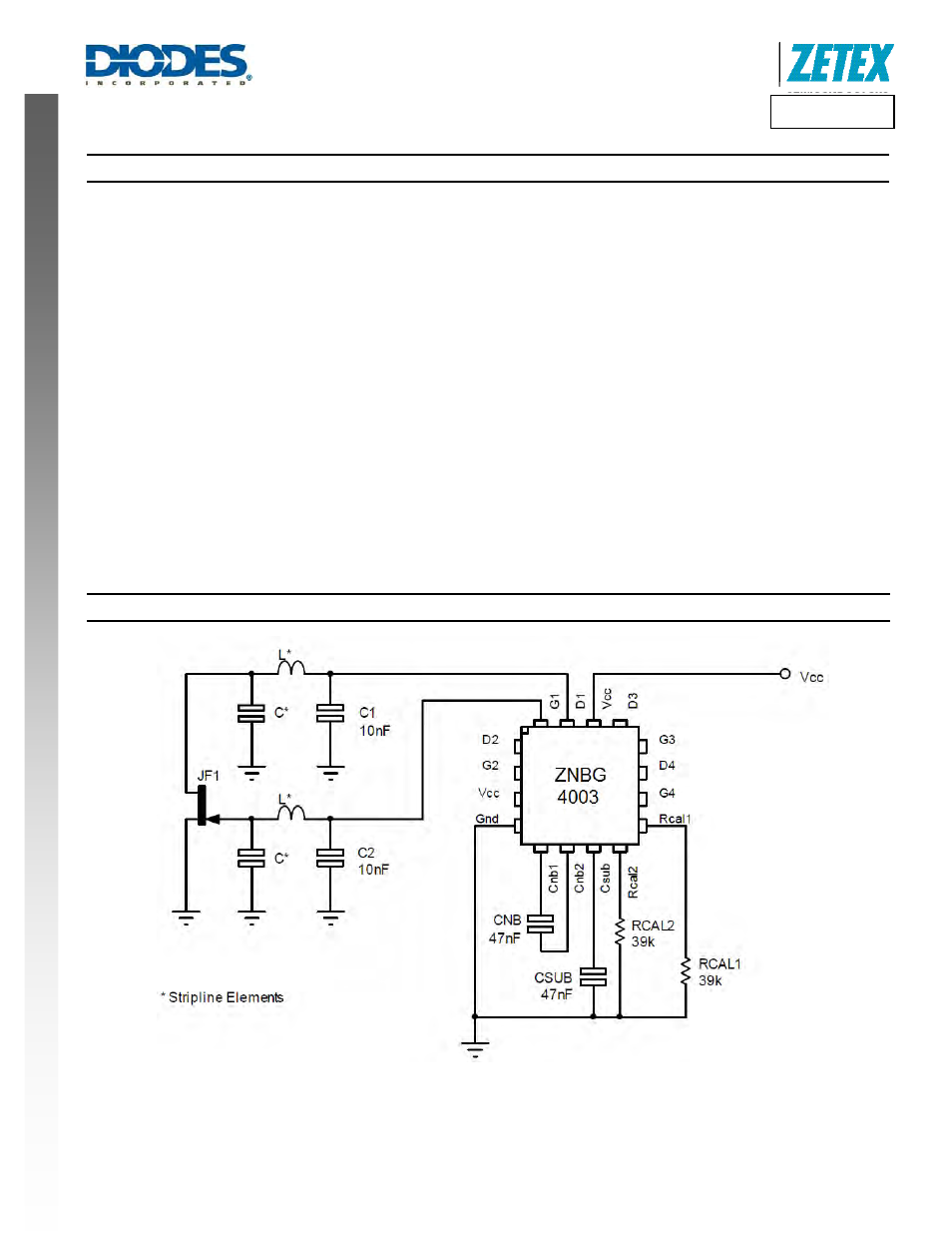
Typical Application Circuit