Functional diagram functional description – Diodes ZNBG6001 User Manual
Page 5
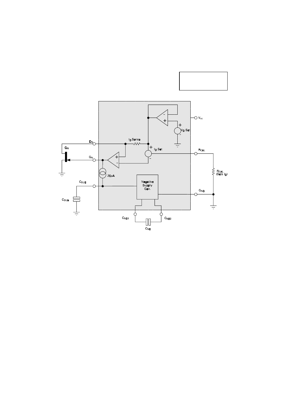
FUNCTIONAL DIAGRAM
FUNCTIONAL DESCRIPTION
The ZNBG devices provide all the bias requirements for external FETs, including the generation
of the negative supply required for gate biasing, from the single supply voltage.
The diagram above shows a single stage from the ZNBG series. The ZNBG4000/1 contains 4 such
stages, the ZNBG6000/1 contains 6. The negative rail generator is common to all devices.
The drain voltage of the external FET Q
N
is set by the ZNBG device to its normal operating voltage.
This is determined by the on board V
D
Set reference, for the ZNBG4000/6000 this is nominally
2.2 volts whilst the ZNBG4001/6001 provides nominally 2 volts.
The drain current taken by the FET is monitored by the low value resistor I
D
Sense. The amplifier
driving the gate of the FET adjusts the gate voltage of Q
N
so that the drain current taken matches
the current called for by an external resistor R
CAL
. Both ZNBG devices have the facility to program
different drain currents into selected FETs. Two R
CAL
inputs are provided. For the ZNBG4000,
resistor R
CAL1
sets the drain current of FETs 1 and 2, resistor R
CAL2
sets the drain current of FETs
3 and 4. For the ZNBG6000, resistor R
CAL1
sets the drain current of FETs 1 and 4, resistor R
CAL2
sets the drain current of FETs 2, 3, 5 and 6.
Since the FET is a depletion mode transistor, it is usually necessary to drive its gate negative with
respect to ground to obtain the required drain current. To provide this capability powered from
a single positive supply, the device includes a low current negative supply generator. This
generator uses an internal oscillator and two external capacitors, C
NB
and C
SUB
.
ZNBG4000
ZNBG4000 ZNBG4001
ZNBG6000 ZNBG6001
4-141