Gate characteristics – Diodes ZNBG6001 User Manual
Page 3
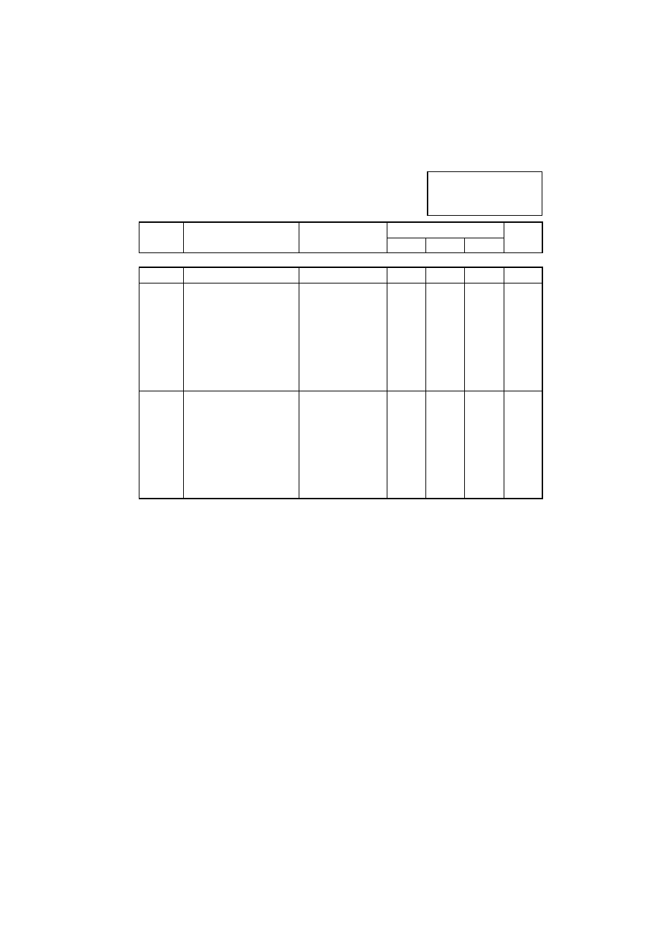
SYMBOL PARAMETER
CONDITIONS
LIMITS
UNITS
Min
Typ
Max
GATE CHARACTERISTICS
I
GO
Output Current Range
-30
2000
µ
A
Output Voltage
ZNBG4000/1
V
OL
Output
Low
I
D1
to I
D4
=12mA
I
G1
to I
G4
=0
-3.5
-2
V
I
D1
to I
D4
=12mA
I
G1
to I
G4
= -10
µ
A
-3.5
-2
V
V
OH
Output High
I
D1
to I
D4
= 8mA
I
G1
to I
G4
= 0
0
1
V
Output Voltage
ZNBG6000/1
V
OL
Output
Low
I
D1
to I
D6
=12mA
I
G1
to I
G6
= 0
-3.5
-2
V
I
D1
to I
D6
=12mA
I
G1
to I
G6
= -10
µ
A
-3.5
-2
V
V
OH
Output High
I
D1
to I
D6
= 8mA
I
G1
to I
G6
= 0
0
1
V
Notes:
1. The negative bias voltages specified are generated on-chip using an internal oscillator. Two external capacitors, C
NB
and C
SUB
, of
47nF are required for this purpose.
2. The characteristics are measured using two external reference resistors R
CAL1
and R
CAL2
of value 33k
Ω
wired from pins R
CAL1/2
to
ground. For the ZNBG4000, resistor R
CAL1
sets the drain current of FETs 1 and 2, resistor R
CAL2
sets the drain current of FETs 3 and 4.
For the ZNBG6000, resistor R
CAL1
sets the drain current of FETs 1 and 4, resistor R
CAL2
sets the drain current of FETs 2, 3, 5 and 6.
3. Noise voltage is not measured in production.
4. Noise voltage measurement is made with FETs and gate and drain capacitors in place on all
outputs. C
G
, 4.7nF, are connected between gate outputs and ground, C
D
, 10nF, are connected
between drain outputs and ground.
ZNBG4000
ZNBG4000 ZNBG4001
ZNBG6000 ZNBG6001
4-139