Diodes ZNBG3211 User Manual
Page 9
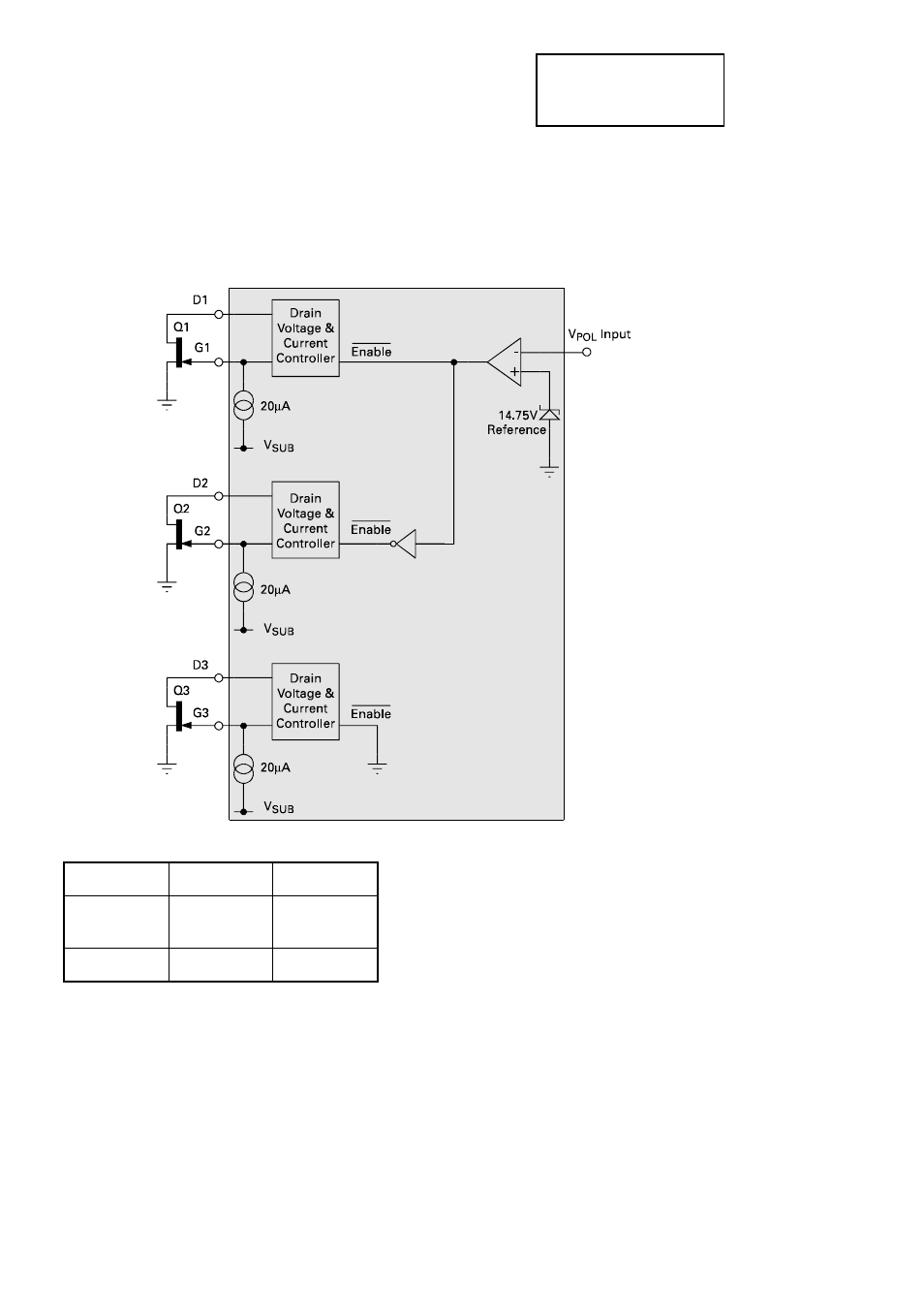
The following schematic shows the function of the V
POL
input. Only one of the two external FETs
numberd Q1 and Q2 are powered at any one time, their selection is controlled by the input V
POL
.
This input is designed to be wired to the power input of the LNB via a high value (10k) resistor.
With the input voltage of the LNB set at or below 14V, FET Q2 will be enabled. With the input
voltage at or above 15.5V, FET Q1 will be enabled. The disabled FET has its gate driven to 0V and
its drain terminal is switched open circuit. FET number Q3 is always active regardless of the
voltage applied to V
POL
.
Control Input Switch Function
Input Sense
Polarisation
Select
⇐⇐≤
14
volts
Vertical
FET Q2
≥
15.5 volts
Horizontal
FET Q1
67-9
ZNBG3210
ZNBG3211
This manual is related to the following products: