Znbg3118, New prod uc t, Applications information – Diodes ZNBG3118 User Manual
Page 8: A product line of diodes incorporated
ZNBG3118
ZNBG3118
Document number: DS32049 Rev. 2 - 2
8 of 10
February 2010
© Diodes Incorporated
NEW PROD
UC
T
A Product Line of
Diodes Incorporated
Applications Information
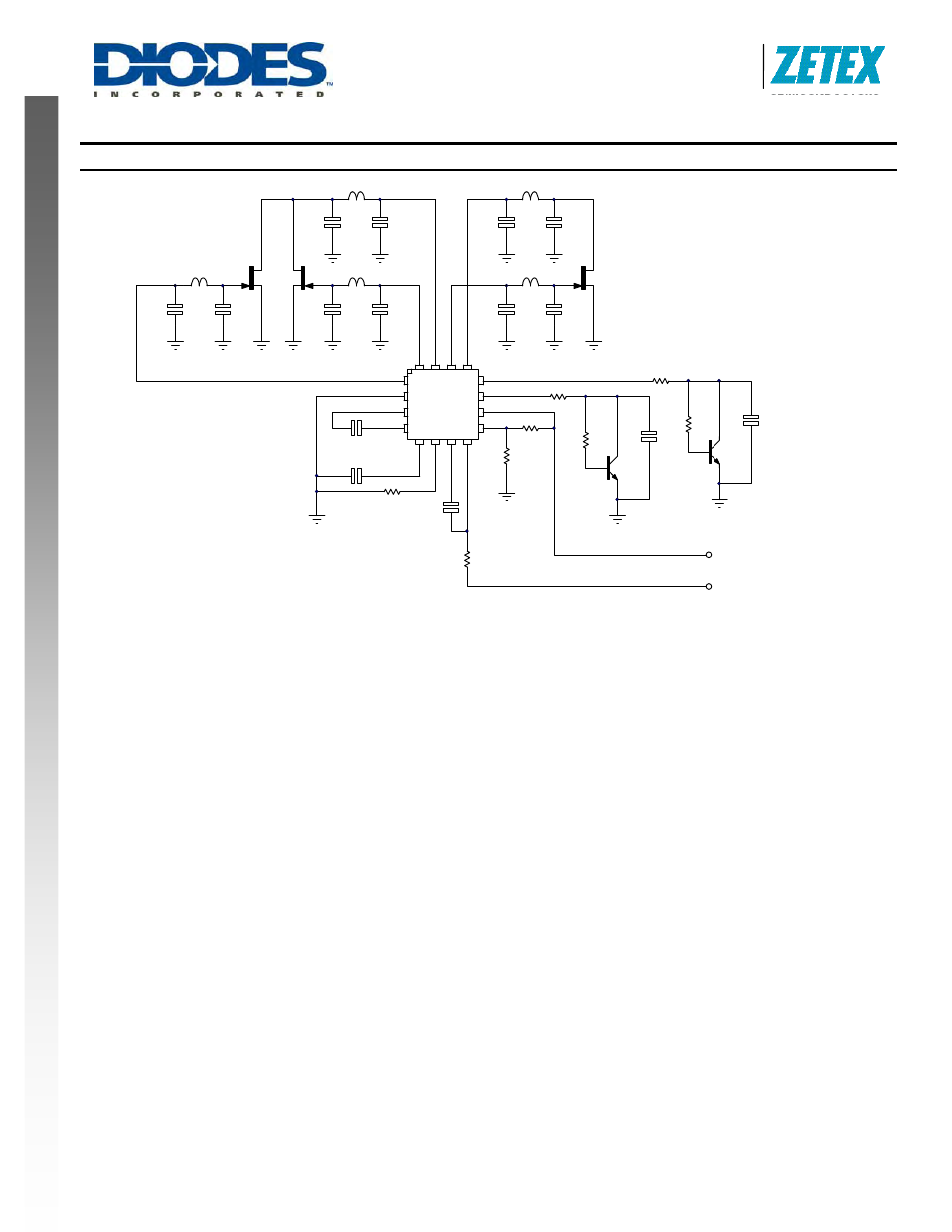
Figure 5 Applications circuit for the ZNBG3118 using Bi-polar local oscillators
Figure 5 is a typical applications circuit for the ZNBG3118, showing all the external components required for appropriate biasing.
The bias circuits are unconditionally stable over the full temperature range with the associated FETs and gate and drain
capacitors in circuit. Capacitors C2, C4, C6, C7 and C9 ensure that residual power supply and substrate generator noise is not
allowed to affect external circuits which may be sensitive to interference. They also serve to suppress any potential RF feed
through between stages via the ZNBG3118. These capacitors are required for all stages used. Values around 10nF are
recommended however this is design dependent and any value between 1nF and 100nF could be used. The capacitor C
SUB
is an
integral part of the ZNBG3118 negative supply generator. The negative bias voltage is generated on-chip using an internal
oscillator. The required value of capacitor C
SUB
is 47nF. This generator produces a low current supply of approximately -2.5V.
Although this generator is intended purely to bias the external FETs, it can be used to power other external low current circuits via
the C
SUB
pin. Note that the exposed pad of the package must be either left floating or connected to Csub.
Resistor R
CAL
sets the drain current at which all external amplifier FETs are operated. To minimize the pin-count and package size
Drain 1 (D1) and Drain 2 (D2) share a common pin. If any bias control circuit is not required, its related drain and gate connections
may be left open circuit without affecting the operation of the remaining bias circuits.
The ZNBG3118 has been designed to protect the external FETs from adverse operating conditions. With a JFET connected to
any bias circuit, the gate output voltage of the bias circuit can not exceed the range -3V under any conditions, including power up
and power down transients. Should the negative bias generator be shorted or overloaded so that the drain current of the external
FETs can no longer be controlled, the drain supply to FETs is shut down to avoid damage to the FETs by excessive drain current.
J2
Vcc
* L2
* C3
* C1
C2
10nF
C4
10nF
CNB 47nF
CSUB 47nF
RLV1
* Stripline Elements
J1
* L3
* C5
C6
10nF
* L1
LNB Downf eed
RPOL
10k
CFIN
330pF
Gnd
ZNBG3118
Csu
b
Cnb1
Cnb2
Rca
l
G2
D3
G3
D1
2
LB
G1
HB
Fi
n
Vpol
Vcc
Lov
J3
* L4
* C10
C9
10nF
C7
10nF
* L3
* C8
RHB1
CHB
RHB2
9.75GHz Local Osc.
10.6GHz Local Osc.
Q4
RLB1
CLB
RLB2
Q5
RLV2
RCAL 39k