Znbg3118, New prod uc t, Local oscillator configurations – Diodes ZNBG3118 User Manual
Page 6: A product line of diodes incorporated
ZNBG3118
ZNBG3118
Document number: DS32049 Rev. 2 - 2
6 of 10
February 2010
© Diodes Incorporated
NEW PROD
UC
T
A Product Line of
Diodes Incorporated
MIMIC local oscillators
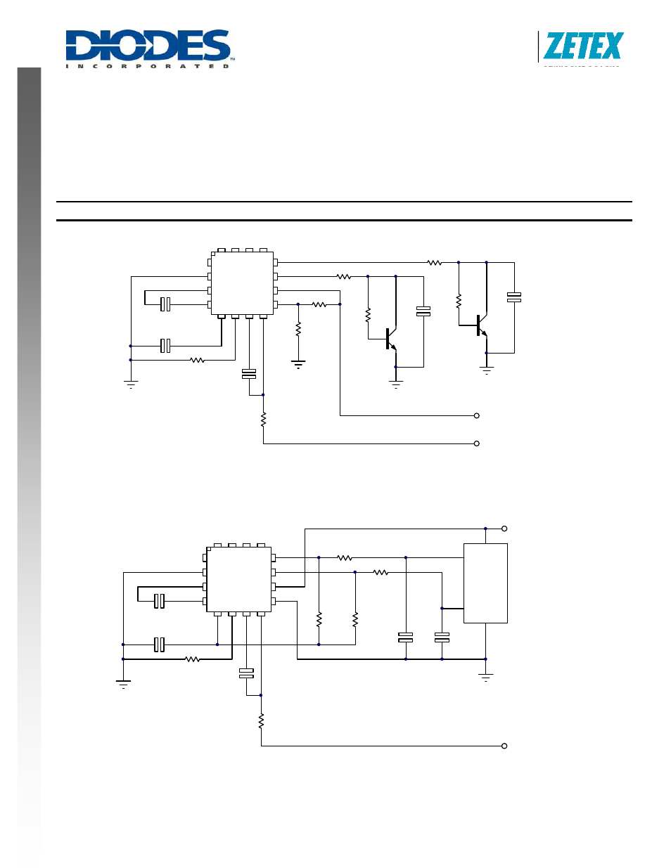
Referring to Figure 3 wiring pin LOV to ground will force LB and HB to switch between -2.5V (disabled) and 0V (enabled). Note
that Vcc(max) should not exceed 6.0V when using this configuration.
Logic enabled PLL local oscillators
Referring to Figure 4 connecting the LOV pin to Vcc will pull the LB and HB to V
CC
when enabled and 0V when disabled. Using the
same supply voltage for the ZNBG3118 and the PLL local oscillator block, the LB and HB outputs will provide a suitable logic signal
of up to 100uA to drive the LO select pin of a PLL system.
Local Oscillator Configurations
Figure 2 Applications circuit for the ZNBG3118 using Bi-polar oscillators
Figure 3 Applications circuit for the ZNBG3118 using MIMIC local oscillators
Vcc
CNB 47nF
CSUB 47nF
RLV1
LNB Downf eed
RPOL
10k
CFIN
330pF
Gnd
ZNBG3118
Csu
b
Cnb1
Cnb2
Rca
l
G2
D3
G3
D1
2
LB
G1
HB
Fi
n
Vpol
Vcc
Lov
RHB1
CHB
RHB2
9.75GHz Local Osc.
10.6GHz Local Osc.
Q1
RLB1
CLB
RLB2
Q2
RLV2
RCAL 39k
Vcc
CNB 47nF
CSUB 47nF
LNB Downf eed
RPOL
10k
CFIN
330pF
Gnd
ZNBG3118
Cs
u
b
Cnb1
Cnb2
Rc
a
l
G2
D3
G3
D1
2
LB
G1
HB
Fi
n
Vp
ol
Vcc
Lov
RHB1
CLB
RLB1
CHB
RCAL 39k
G2
G1
Local
Osc.
MMIC
RHB2
240k
RLB2
240k