Dc test circuits – Diodes ZTL432 User Manual
Page 6
ZTL431/ZTL432
Document number: DS33263 Rev. 16 - 2
6 of 10
May 2013
© Diodes Incorporated
A Product Line of
Diodes Incorporated
ZTL431/ZTL432
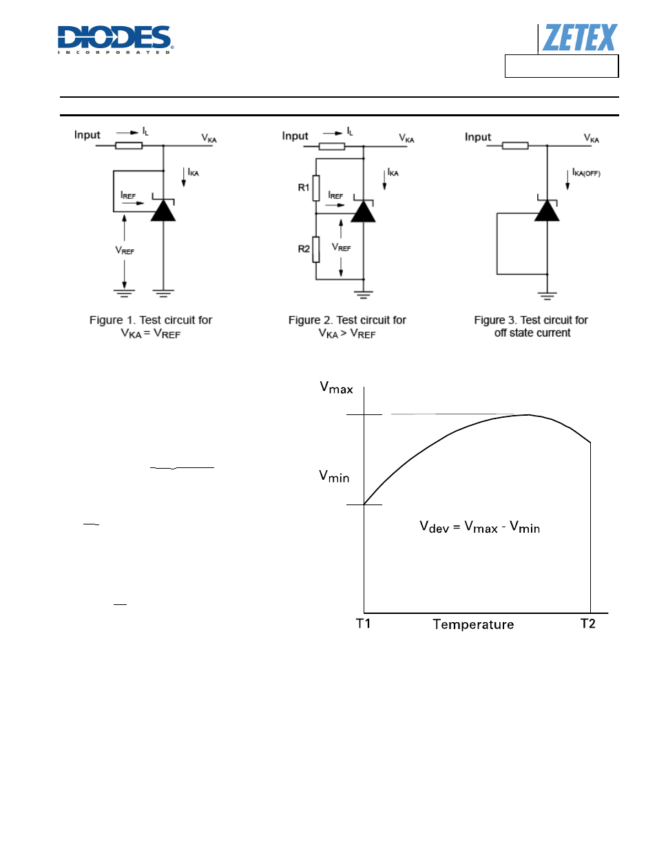
DC Test Circuits
Notes
Deviation of reference input voltage, Vdev, is defined as the
maximum variation of the reference input voltage over the full
temperature range.
The average temperature coefficient of the reference input
voltage, V
REF
is defined as:
V
REF
(ppm/°C) = V
DEV
1,000,000
V
REF
(T1-T2)
The dynamic output impedance, R
z
, is defined as:
R
Z
= ΔV
Z
ΔI
Z
When the device is programmed with two external resistors, R1
and R2, (figure 2), the dynamic output impedance of the overall
circuit, R'
z
, is defined as:
R'
Z
= R
Z
(1 + R1 )
R2
Stability Boundary
The ZTL431 and ZTL432 are stable with a range of capacitive
loads. A zone of instability exists as demonstrated in the typical
characteristic graph on page 4. The graph shows typical
conditions. To ensure reliable stability a capacitor of 4.7nF or
greater is recommended between anode and cathode.