Pin description, Function block diagram – Diodes ZXRE060 User Manual
Page 2
ZXRE060
0.6V ADJUSTABLE PRECISION SHUNT REGULATOR
ZXRE060
Document number: DS33611 Rev. 6 - 2
2 of 12
March 2011
© Diodes Incorporated
A Product Line of
Diodes Incorporated
Pin Description
Pin
(SC70-5 /SOT353,
TSOT23-5)
Pin
(DFN)
Name
Function
1 1
PGND
Power Ground: Ground return for emitter of output transistor: Connect PGND and
GND together.
- 2
No
connection
5 3
OUT
Output. Connect a capacitor close to device between OUT and GND. See the
Applications Information section.
4
4
FB
Feedback Input. Regulates to 600mV nominal.
2 5
GND
Analog Ground: Ground return for reference and amplifier: Connect GND and
PGND together.
3 6
IN
Supply Input. Connect a 0.1
μF ceramic capacitor close to the device from IN to
GND.
-
Flag
Floating or connect to GND
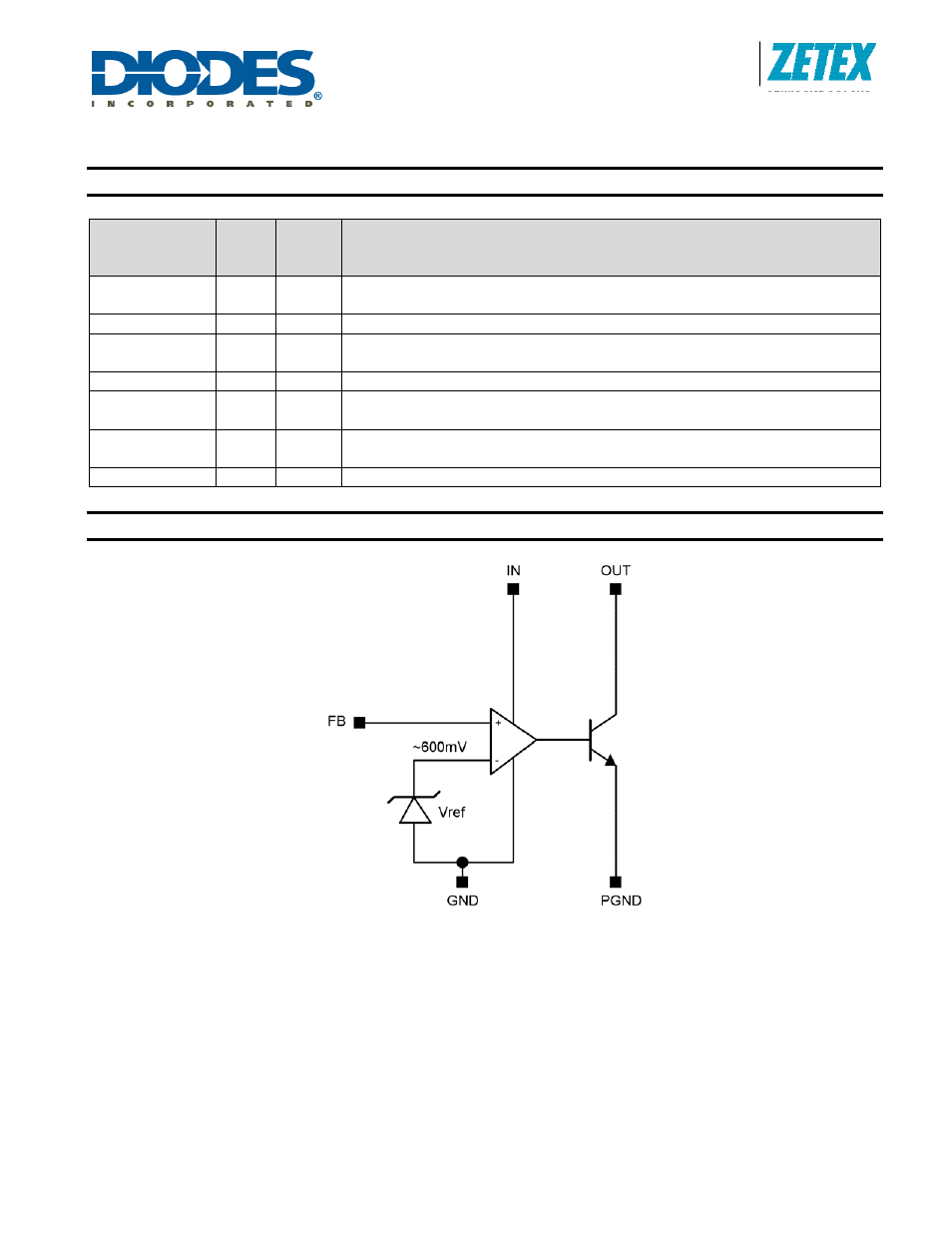
Function Block Diagram
The ZXRE060 differs from most other shunt regulators in that it has separate input and output pins and a low voltage reference.
This enables it to regulate rails down to 600mV and makes the part ideal for isolated power supply applications that use opto-
couplers in the feedback loop and where the open-collector output is required to operate down to voltages as low as 200mV.
The wide input voltage range of 2V to 18V and output voltage range of 0.2V to 18V enables the ZXRE060 to be powered from
an auxiliary rail, while controlling a master rail which is above the auxiliary rail voltage, or below the minimum V
IN
voltage. This
allows it to operate as a low-dropout voltage regulator for microprocessor/DSP/PLD cores.
As with other shunt regulators (and shunt references), the ZXRE060 compares its internal amplifier FB pin to a high accuracy
internal reference; if FB is below the reference then OUT turns off, but if FB is above the reference then OUT sinks current – up
to a maximum of 15mA.