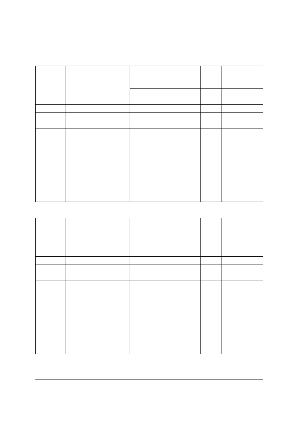
Zsr series, Zsr500 test conditions (unless otherwise stated):t, 25°c, i – Diodes ZSR SERIES User Manual
Page 4: 100ma, v
ZSR SERIES
© Zetex Semiconductors plc 2007
ZSR500 test conditions (Unless otherwise stated):T
j
=25°C, I
O
=100mA, V
in
=9V
ZSR800 test conditions (Unless otherwise stated):T
j
=25°C, I
O
=100mA, V
in
=12V
NOTES:
(
)T
j
=-55 to 125°C
Symbol
Parameter
Conditions
Min.
Typ.
Max.
Units
V
O
Output Voltage
4.875
5
5.126
V
I
O
=1 to 200mA
(
)
4.8
5.2
V
V
in
=7 to 20V
I
O
=1 to 100mA
(
)
4.8
5.2
V
⌬V
O
Line regulation
V
in
=7 to 20V
10
40
mV
⌬V
O
Load regulation
I
O
=1 to 200mA
5
25
mV
I
O
=1 to 100mA
2
mV
I
g
Quiescent current
(
)
350
600
A
⌬I
g
Quiescent current change I
O
=1 to 200mA
100
A
V
in
=7 to 20V
100
A
V
n
Output noise voltage
f=10Hz to 10Hz
75
V rms
⌬V
in
/
⌬V
O
Ripple rejection
V
in
=8 to 18V
48
62
dB
f=120Hz
V
in
Input voltage required to
maintain regulation
7
6.7
V
⌬V
O
/
⌬T
Average temperature
coefficient of V
O
I
O
=5.0mA
(
)
0.1
mV/°C
Symbol
Parameter
Conditions
Min.
Typ.
Max.
Units
V
O
Output Voltage
7.8
8
8.25
V
I
O
=1 to 200mA
(
)
7.68
8.32
V
V
in
=10 to 20V
I
O
=1 to 100mA
(
)
7.68
8.32
V
⌬V
O
Line regulation
V
in
=10 to 20V
11
40
mV
⌬V
O
Load regulation
I
O
=1 to 200mA
8
30
mV
I
O
=1 to 100mA
3
mV
I
g
Quiescent current
(
)
350
600
A
⌬I
g
Quiescent current change I
O
=1 to 200mA
100
A
V
in
=10 to 20V
100
A
V
n
Output noise voltage
f=10Hz to 10Hz
115
V rms
⌬V
in
/
⌬V
O
Ripple rejection
V
in
=11 to 18V
44
60
dB
f=120Hz
V
in
Input voltage required to
maintain regulation
9.7
V
⌬V
O
/
⌬T
Average temperature
coefficient of V
O
I
O
=5.0mA
(
)
0.25
mV/°C