Zxct1011 – Diodes ZXCT1011 User Manual
Page 5
ZXCT1011
© Zetex Semiconductors plc 2005
Pin description
Application information
Design example
The following lines describe how to scale a load current to an output voltage.
V
sense
= (V
sense+
) - (V
sense-
) = I
load
x R
sense
Defining then
I
out
= Iq + V
sense
x g
m
since g
m
= 1.2 / R
shunt
I
out
= Iq + [ (V
sense
x 1.2) / R
shunt
]
= Iq + [ (1.2 x I
load
x R
sense
/ R
shunt
) ]
Note: Iq is embedded into the specification of the ZXCT1011 and therefore appears an offset error.
∴
V
out
= (R
out
x I
offset
) + [(1.2 x R
out
x I
load
x R
sense
) / R
shunt
]
The output current of the ZXCT1011 is directly related to the size of the trimming resistor used. It
is important to ensure the tolerance of R
shunt
is considered. A 1% change in R
shunt
will cause a
1% change in output.
Consider the following: -
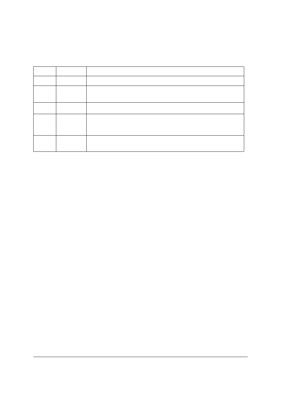
Pin no.
Pin name
Pin function
1
N/C
No connection
2
I
out
Output current - follows transconductance of sense voltage g
m
= 10mA/V
for R
shunt
=120
⍀
3
R
shunt
Trimming resistor Input. - used to trim gain value 60
⍀
Յ
R
shunt
Յ
240
⍀
4
V
sense-
Low side current sense input. – connect to load/battery etc. Must be
lower than V
sense+
for correct operation. Cannot be grounded
without additional series resistor.
5
V
sense+
High side current sense input. – Connect to supply rail. Must be
higher than V
sense+
for correct operation.