Zxld1370, Absolute maximum ratings, Package thermal data – Diodes ZXLD1370 User Manual
Page 4
ZXLD1370
Document number: DS32165 Rev. 5 - 2
4 of 39
September 2012
© Diodes Incorporated
ZXLD1370
A Product Line of
Diodes Incorporated
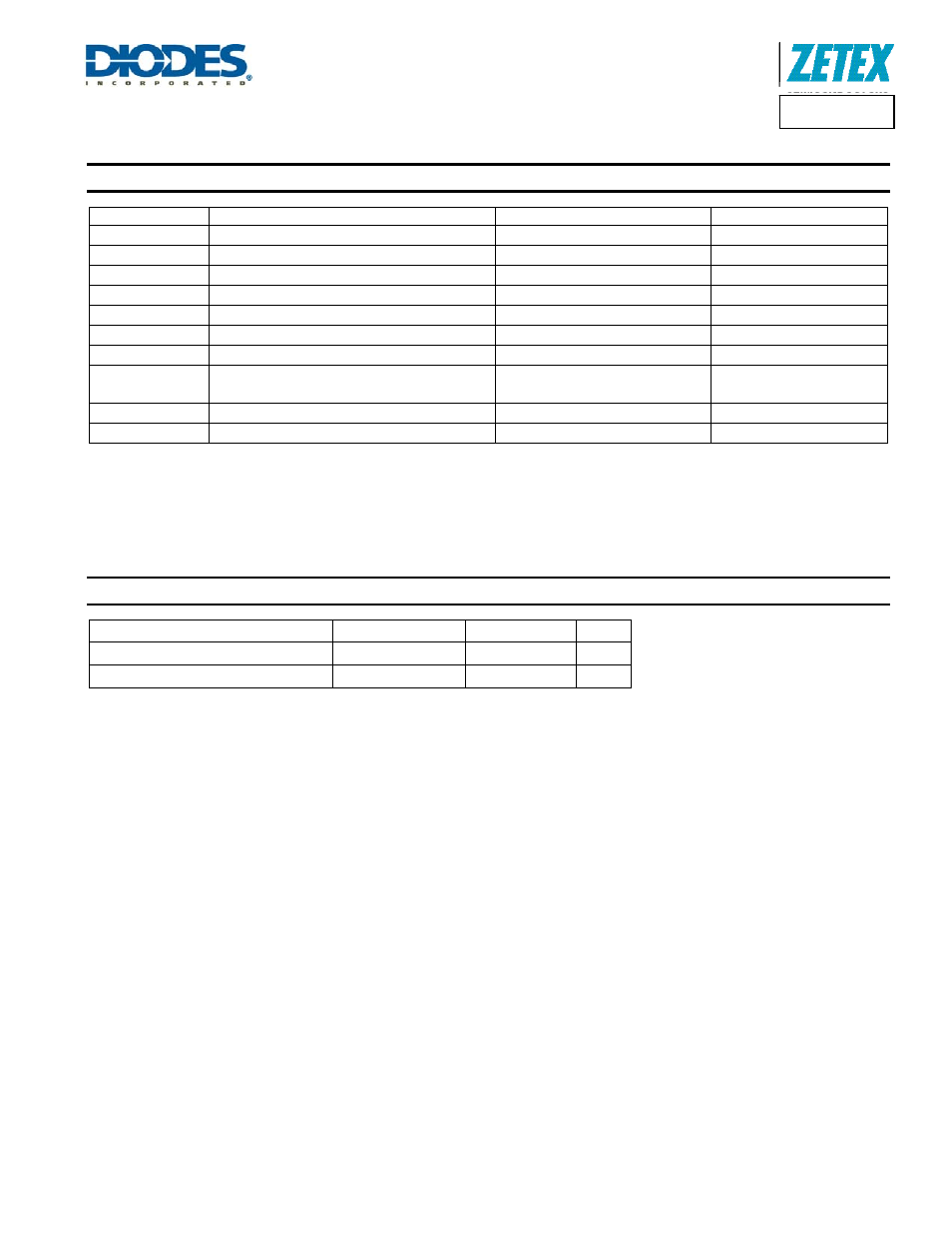
Absolute Maximum Ratings
(Note 5) (Voltages to GND, unless otherwise specified.)
Symbol Parameter
Rating
Unit
V
IN
Input Supply Voltage Relative to GND
-0.3 to +65
V
V
AUX
Auxiliary Supply Voltage Relative to GND
-0.3 to +65
V
V
ISM
Current Monitor Input Relative to GND
-0.3 to +65
V
V
SENSE
Current Monitor Sense Voltage (V
IN
-V
ISM
)
-0.3 to +5
V
V
GATE
Gate Driver Output Voltage
-0.3 to +20
V
I
GATE
Gate Driver Continuous Output Current
18
mA
V
FLAG
Flag Output Voltage
-0.3 to 40
V
V
PWM
, V
ADJ
,
V
TADJ
, V
GI
Other Input Pins
-0.3 to +5.5
V
T
J
Maximum Junction Temperature
150
°C
T
ST
Storage Temperature
-55 to +150
°C
Stresses greater than the 'Absolute Maximum Ratings' specified above, may cause permanent damage to the device. These are stress ratings only; functional
operation of the device at these or any other conditions exceeding those indicated in this specification is not implied. Device reliability may be affected by exposure to
absolute maximum rating conditions for extended periods of time.
Semiconductor devices are ESD sensitive and may be damaged by exposure to ESD events. Suitable ESD precautions should be taken when handling and
transporting these devices.
Package Thermal Data
Thermal Resistance
Package
Typical
Unit
Junction-to-Ambient, θ
JA
(Note 6)
TSSOP-16EP 50
°C/W
Junction-to-Case, θ
JC
TSSOP-16EP 23
°C/W
Notes: 5.
For
correct operation SGND and PGND should always be connected together.
6. Measured on High Effective Thermal Conductivity Test Board" according JESD51.