Zxld1350, Application information (continued), Layout considerations – Diodes ZXLD1350 User Manual
Page 20
ZXLD1350
30V 350mA LED DRIVER with AEC-Q100
ZXLD1350
Document number: DS33468 Rev. 8 - 2
20 of 22
March 2011
© Diodes Incorporated
A Product Line of
Diodes Incorporated
Application Information (Continued)
Layout considerations
LX pin
The LX pin of the device is a fast switching node, so PCB tracks should be kept as short as possible. To minimize ground
'bounce', the ground pin of the device should be soldered directly to the ground plane.
Coil and decoupling capacitors
It is particularly important to mount the coil and the input decoupling capacitor close to the device to minimize parasitic
resistance and inductance, which will degrade efficiency. It is also important to take account of any track resistance in series
with current sense resistor RS.
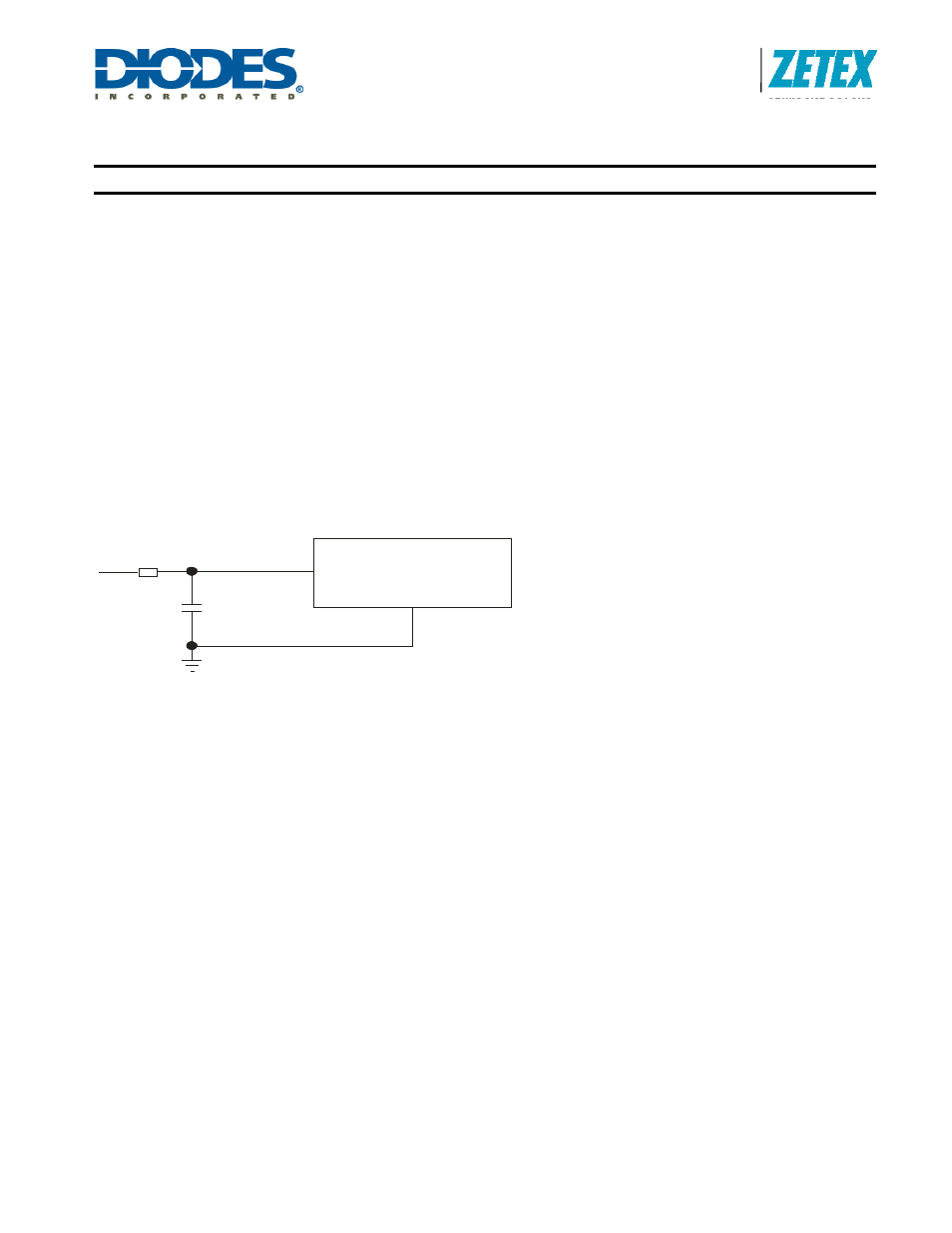
ADJ pin
The ADJ pin is a high impedance input, so when left floating, PCB tracks to this pin should be as short as possible to reduce
noise pickup. A 100nF capacitor from the ADJ pin to ground will reduce frequency modulation of the output under these
conditions. An additional series 10k
Ω resistor can also be used when driving the ADJ pin from an external circuit (see below).
This resistor will provide filtering for low frequency noise and provide protection against high voltage transients.
ZXLD1350
GND
ADJ
100nF
GND
10k
High voltage tracks
Avoid running any high voltage tracks close to the ADJ pin, to reduce the risk of leakage due to board contamination. Any
such leakage may raise the ADJ pin voltage and cause excessive output current. A ground ring placed around the ADJ pin
will minimize changes in output current under these conditions.