Application information (continued) – Diodes ZXLD1350 User Manual
Page 13
ZXLD1350
30V 350mA LED DRIVER with AEC-Q100
ZXLD1350
Document number: DS33468 Rev. 8 - 2
13 of 22
March 2011
© Diodes Incorporated
A Product Line of
Diodes Incorporated
Application Information (Continued)
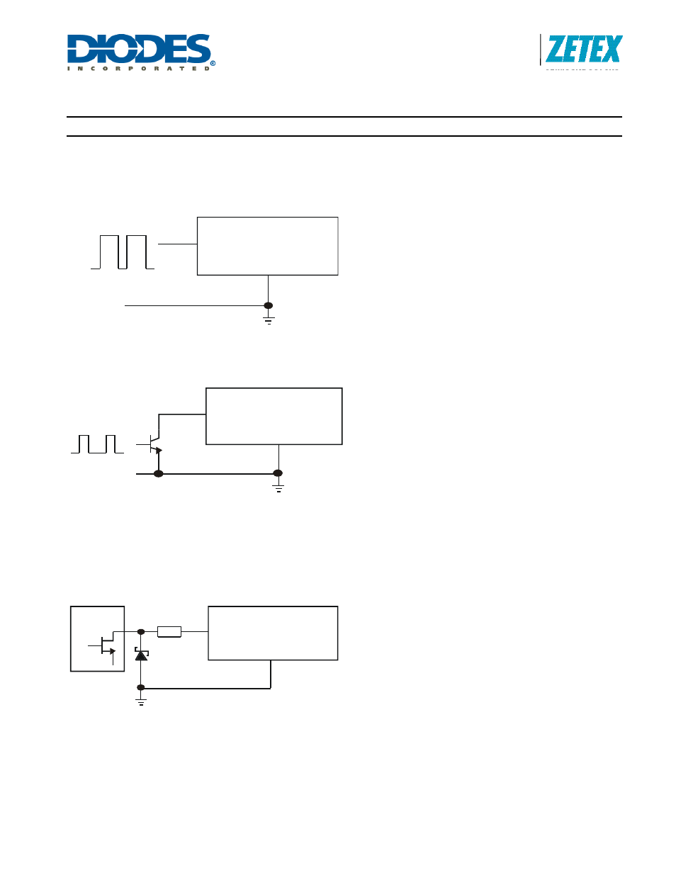
Output Current Adjustment by PWM Control
Directly driving ADJ input
A Pulse Width Modulated (PWM) signal with duty cycle D
PWM
can be applied to the ADJ pin, as shown below, to adjust the
output current to a value above or below the nominal average value set by resistor R
S
:
Driving the ADJ input via open collector transistor
The recommended method of driving the ADJ pin and controlling the amplitude of the PWM waveform is to use a small NPN
switching transistor as shown below:
This scheme uses the 200k resistor between the ADJ pin and the internal voltage reference as a pull-up resistor for the
external transistor.
Driving the ADJ input from a microcontroller
Another possibility is to drive the device from the open drain output of a microcontroller. The diagram below shows one
method of doing this:
The diode and resistor suppress possible high amplitude negative spikes on the ADJ input resulting from the drain-source
capacitance of the FET. Negative spikes at the input to the device should be avoided as they may cause errors in output
current, or erratic device operation.
PWM dimming can be further split into high frequency and low frequency PWM dimming and how the device responds to
these.
V
ADJ
GND
ADJ
ZXLD1350
GND
0V
PWM
ADJ
ZXLD1350
GND
GND
PWM
ZXLD1350
GND
ADJ
10k
MCU