Zxld1352, Electrical characteristics – Diodes ZXLD1352 User Manual
Page 4
ZXLD1352
ZXLD1352
Document number: DS33469 Rev. 3 - 2
4 of 21
December 2010
© Diodes Incorporated
A Product Line of
Diodes Incorporated
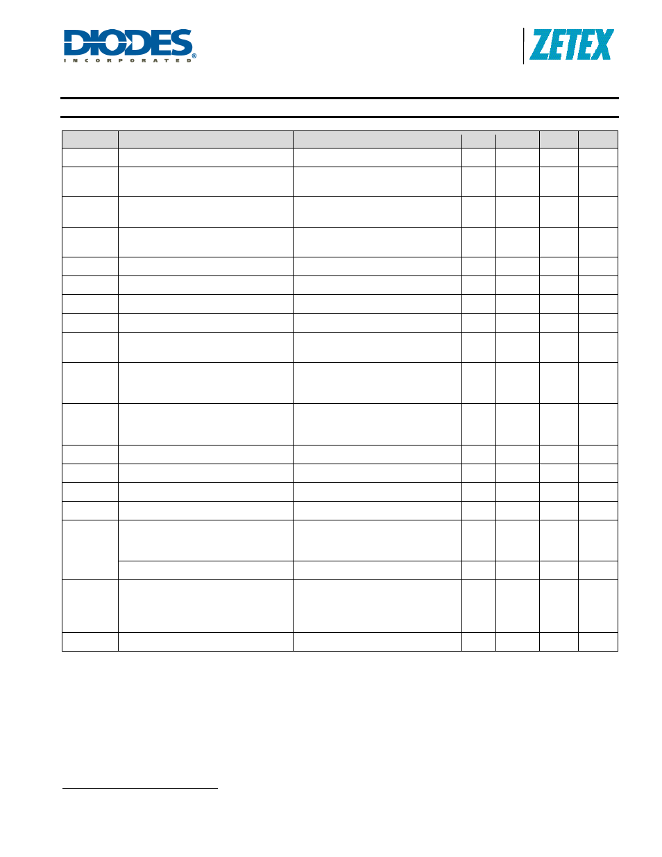
Electrical Characteristics
(Test conditions: V
IN
= 12V, T
amb
= 25°C, unless otherwise specified.)
Symbol
Parameter
Conditions
Min.
Typ.
Max.
Unit
V
SU
Internal regulator start-up threshold
V
IN
rising
4.8
V
I
INQoff
Quiescent supply current
with output off
ADJ pin grounded
20
30
µA
I
INQon
Quiescent supply current
with output switching
ADJ pin floating
f = 250kHz
250
500
µA
V
SENSE
Mean current sense threshold voltage
(defines LED current setting accuracy)
Measured on I
SENSE
pin with respect
to V
IN
V
ADJ
=1.25V
95 100 105 mV
V
SENSEHYS
Sense threshold hysteresis
±15
%
I
SENSE
I
SENSE
pin input current
V
SENSE
= V
IN
-0.1
1.25
10
µA
V
REF
Internal reference voltage
Measured on ADJ pin with pin floating
1.21
1.25
1.29
V
ΔV
REF
/
ΔT Temperature coefficient of V
REF
50
ppm/°C
V
ADJ
External control voltage range on ADJ
pin for dc brightness control
1
0.3
2.5
V
V
ADJoff
DC voltage on ADJ pin to switch device
from active (on) state to quiescent (off)
state
V
ADJ
falling
0.15
0.2
0.25
V
V
ADJon
DC voltage on ADJ pin to switch device
from quiescent (off) state to active (on)
state
V
ADJ
rising
0.2
0.25
0.3
V
R
ADJ
Resistance between ADJ pin and V
REF
35
65
k
Ω
I
LXmean
Continuous LX switch current
0.37
A
R
LX
LX Switch ‘On’ resistance
1.5
2
Ω
I
LX(leak)
LX switch leakage current
1
µA
D
PWM(LF)
Duty cycle range of PWM signal
applied to ADJ pin during PWM
dimming mode
PWM frequency 100Hz – 1kHz
PWM amplitude = V
REF
Measured on ADJ pin
0.001
1
Brightness control range
1000:1
f
LX
Operating frequency
(See graphs for more detail)
ADJ pin floating
L=100µH (0.82V)
I
OUT
=350mA @ V
LED
=3.4V
Driving 1 LED
250 kHz
t
PD
Internal comparator propagation delay
50
ns
Notes:
1. Production testing of the device is performed at 25°C. Functional operation of the device and parameters specified over a -40°C to +105°C temperature
range, are guaranteed by design, characterization and process control.
2. 100% brightness corresponds to VADJ = VADJ(nom)
= VREF. Driving the ADJ pin above V
REF
will increase the VSENSE threshold and output current
proportionally.